
2.2. Fundamentals of Signal Amplification: The Linear Circuit
The most fundamental property of a useful electronic voltage amplification device is that it possess a transconductance that leads to the possibility of voltage gain. Transconductance is defined as the ratio of the signal (ac, incremental) current out, iout ≡ δiOUT, and the applied input signal voltage, vin ≡ δvIN. That is, transconductance gm is
Equation 2.3
![]()
For the BJT, iOUT ≡ iC and vIN ≡ vBE, while for the NMOS, iOUT ≡ iD and vIN ≡ vGS. Thus, (2.1) and (2.2) can be used for the BJT and MOSFET, respectively, to obtain an expression for gm. The results are
Equation 2.4
![]()
and
Equation 2.5
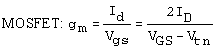
IC and ID are the dc (bias) currents of the transistors, so for comparison they can be made equal. At room temperature, the thermal voltage is VT = 26 m. For the MOSFET, VGS is the gate – source bias voltage and Vtn is the transistor threshold voltage. The difference, as in the denominator of the transconductance expression, could typically be about VGS – Vtn = 500 mV.
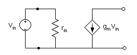
The expression (2.3) suggests the linear model given in Fig. 2.2. Included in the model is an input resistance, rin, which accounts for the fact that there can be an incremental current flowing into the input terminal for an increment of input voltage. The model applies in general to amplifying devices, including the vacuum tube (VT), BJT, JFET, and MOSFET. There exists a wide range of magnitude of transconductance and input resistance between the devices. The input resistance, though, affects only the loading of the input signal source; otherwise, the relation of (2.3) applies in all cases, and the transconductance is the key to the gain for a given device type. The input resistance is essentially infinite for the vacuum tube and the MOSFET (common source) but can be as low as a few ohms in some configurations for the BJT (e.g., common base).
Figure 2.2. Basic linear model of a voltage amplification device. Model parameters are gm and rin.
It is interesting to compare the transconductance of the BJT and MOSFET along with the vacuum tube. We will make a comparison at ID = IC = 10 mA (suitable for a vacuum tube) even though transistors would not usually be operated at such high currents, especially in an integrated circuit. Consulting a source of information for a triode 6SN7 (perhaps one of the most common tubes of all time), one deduces from a graphical analysis the plate characteristics that, for example, gm(VT) = 3 mA/V. From (2.4) and (2.5), we obtain gm(BJT) = 385 mA/V and gm(MOSFET) = 40 mA/V with VGS – Vtn = 500 mV. The BJT is decidedly superior in this respect, and this is one of the factors contributing to the sustained life of the transistor in industry. That is, the BJT amplifier stage can potentially have a much higher voltage gain. The vacuum tube is clearly inferior to both transistors and points to the reason for the need for so many amplification stages in some VT amplifiers.
The output voltage of amplifiers based on any of the devices will depend on the value of the load resistance, RL, which is added to the circuit of Fig. 2.2 in Fig. 2.3. Note that, in general, RL is not necessarily an actual resistor but could be an effective resistance, as dictated by the amplifier circuitry that is connected to the output of a given stage, combined with a bias resistor. The output voltage induced across RL will be
Equation 2.6
![]()
Figure 2.3. Basic linear model of a voltage amplification device with load RL connected.

The minus sign is a result of the current flowing up through RL. The signal voltage gain is the incremental output voltage divided by the incremental input voltage such that the gain can readily be obtained from (2.6) as
Equation 2.7
![]()
Thus, the gain is directly related to the parameter gm for a given transistor. In general, av can be positive or negative, depending on the terminal configuration. For example, the common base (BJT) and common gate (MOSFET) are positive (noninverting) gain amplifiers.