
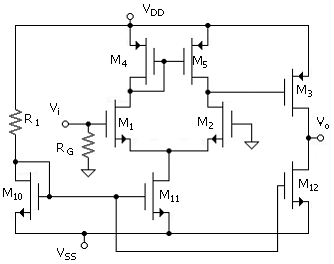
14.5. Two-Stage Amplifier with Current-Source Biasing
The cascade amplifier that includes all features discussed up to this point is given in Fig. 14.5. Note that the only (internal) resistor is that of the reference-current circuit. Bias currents for this circuit can be set up using gate-width proportions. We note that ID3 ∝ ID5 since M3 and M5 have a common bias voltage, VSG4. Thus
Equation 14.24
![]()
Figure 14.5. Two-stage amplifier with current-source biasing. R1 is the only resistor in the internal circuit. RG is externally connected.
Also, M11 and M12 are referred to the same reference voltage such that
Equation 14.25
![]()
Using ID3 = ID12 and ID11 = 2ID5, we obtain
Equation 14.26
![]()
Combining (14.24) and (14.26) leads to
Equation 14.27
![]()
Assume that W11 has been picked to satisfy the design ID11. W12 is then selected to give the design ID12 using ID12/ID10 = W12/W10. W5 is selected on the basis of signal considerations. This leaves the computation of W3 [from (14.27)].
A precision calculation includes the lambda effects and is from
Equation 14.28
![]()
The simple form should normally suffice. The dc output voltage VO is very sensitive to some of the parameters and the approximate calculation from (14.27) will not result in VO = 0. However, uncertainties in transistor parameters preclude the justification of using (14.28) in practice.
The overall signal gain is now obtainable using (14.17) for the differential stage and (14.8) for the common-source stage with a current-source load. The result is
Equation 14.29
![]()
A useful form for making a quantitative gain assessment is
Equation 14.30
![]()
Based on the same parameters as used previously for gain calculations (λn = λp = 1/20 V and Veffn = Veffp = 0.3 V), the gain magnitude is 4440. The value compares with 116 for the all-resistor circuit for Fig. 13.1 and 289 for the circuit of Fig. 14.3. In this special case, both stages contribute the same value.