
4.1. Amplifier Circuit and Signal Equivalent Circuits
To serve as an illustration of the utility of the parameters, the discussion of the linear model and g parameters will be accompanied by a signal-performance evaluation of an NMOS transistor in the most general amplifier configuration (Fig. 4.1). The circuit includes drain and source resistors, and input is at the gate terminal. As shown in Fig. 4.1(b), output can be at the drain (common-source amplifier) or source (source-follower amplifier).
Figure 4.1. (a) Ideal NMOS in a basic common-source amplifier circuit (output, Vocs). Dc supply nodes of Fig. 4.1(a) are set to zero volts to obtain the signal circuits of Fig. 4.1(b) and (c). An alternative output is Voef [shown in (b)], which is the source-follower amplifier stage. Voltage variable Vg is the input for both cases.
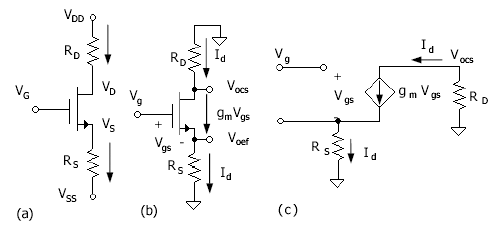
Figure 4.1 shows the dc (bias) circuit (a) and signal circuit (b). Replacing all dc nodes with signal ground and replacing the dc variables with signal variables as in Fig. 4.1 produces the signal circuit. It will be assumed that the schematic symbol for the transistor in signal circuit (b) is equivalent to the ideal, intrinsic linear model of the transistor. The total drain current of the model is Id = gmVgs, as, for example, in the basic circuit of Fig. 2.4. The linear equivalent model is that of Fig. 4.1(c). The symbolic transistor in Fig. 4.1(b) is more intuitively representative in terms of the overall circuit perspective than that of Fig. 4.1(c). For this reason, the Fig. 4.1(b) version is chosen for use in all of the following discussions of MOSFET circuits. All other details of the transistor model, as discussed in this unit, will be added externally.
Signal Vg = Vi is applied to the gate (input) and, in response, a signal voltage, Vo, appears at the drain (or source). We would like to analyze the signal performance in terms of voltage gain, av = Vo/Vi = Vd/Vg (or av = Vs/Vg), of the circuit based on a linear (small-signal) analysis. In any case, the voltage gain is av = GmRx, where Gm is the circuit transconductance (as opposed to the transistor transconductance) and x = D (common source) or x = S (source follower). Thus, the goal will be to obtain a relation for Gm for a given linear model of the transistor. Circuit transconductance is determined in the following for models with the various parameters included.