
6.1. Grounded-Source Amplifier: Coupling Capacitor
A version of the circuits of Fig. 5.2, as given in Fig. 6.1, is generalized to include a resistance, Rs, as part of the input signal source. The input signal at the gate (and thus the output) will fall off for decreasing frequencies as the magnitude of reactance of the capacitor increases. The value of the capacitor is selected such that the reactance will be small compared to the value of the sum of the resistors, at the lowest operating frequency.
Figure 6.1. Circuit with coupling capacitor. Capacitor blocks the signal at low frequencies. Cg and RG = RG1 || RG2 must be selected for | XCg | <<Rs + RG at the gain measurement frequency.
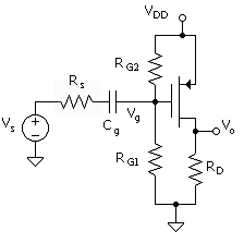
In this amplifier, all the gain-frequency dependence is between Vg and Vs. The relation between the gate signal, Vg, and source signal, Vs, based on a voltage-divider relation is
Equation 6.1

with
Equation 6.2
![]()
where RG = RG1 || RG2.
With Rs included, the f3dB expression applies to an actual amplifier. In Project 6, the signal-source voltage is applied directly to the gate. We select a combination of RG and Cg to obtain a suitably low f3dB. This must be more than a factor of 10 lower than the gain measurement frequency assure that the capacitor is not influencing the measurements.
In Projects 5 and 7, no capacitor is used at the input as the signal is superimposed on the dc gate voltage. This is to facilitate the need for both DAQ output channels to provide the bias. However, Project 6, one channel provides the bias, as in Figs. 5.1(a) and 6.1, and the other channel is used for the signal with connection to the input through a coupling capacitor.