
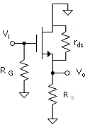
7.2. Source-Follower Voltage Transfer Relation
A signal circuit is shown in Fig. 7.2, where the dc supplies have been replaced with ground. Also, the internal resistance, rds = 1/gds, of the transistor has been included in the signal circuit. Note that it is in parallel with RS since the drain is tied to signal ground. Assume for now that source and body are connected as in Fig. 7.1.
Figure 7.2. Signal circuit of the source follower. Body effect is absent since the source and body are assumed connected.
Regardless of the terminal configuration, for infinite output resistance and with the body and source connected, the relationship between the drain current and gate – source control voltage of the transistor is (4.1) with gds = gmb = 0, which is [(2.5)]
![]()
In the source-follower circuit, the output resistance of the transistor can be included in the source-follower load and (2.5) effectively applies.
The transconductance for the circuit configuration with a source resistor was shown in Unit 4 to be [(4.8)]
![]()
where, for this case, ![]() is the source-follower load, which includes the transistor output resistance and is
is the source-follower load, which includes the transistor output resistance and is
Equation 7.3
![]()
Then using
Equation 7.4
![]()
the “gain” (the transfer function is less than unity) is determined to be
Equation 7.5
![]()
Ideally, this is a unity gain, as would be the case for ![]() . In bipolar transistors, this condition is closely approached. However, in MOSFET source followers, the ideal case is in general not reached. As we will see below, this deficiency is enhanced when the body effect is included.
. In bipolar transistors, this condition is closely approached. However, in MOSFET source followers, the ideal case is in general not reached. As we will see below, this deficiency is enhanced when the body effect is included.
Note that av is
Equation 7.6

This is the expression for a simple voltage divider. Thus the source follower is the equivalent of a unity-gain circuit with load ![]() and output resistance 1/gm. We can conclude that the transistor viewed from the source has an output resistance of 1/gm.
and output resistance 1/gm. We can conclude that the transistor viewed from the source has an output resistance of 1/gm.
Finally, with ![]() separated into its component parts, the source-follower gain becomes
separated into its component parts, the source-follower gain becomes
Equation 7.7

In general, the gds parameter can be dropped. The ratio of gm/gds is
Equation 7.8
![]()