
5.2. Amplifier Voltage Gain
This dc (bias) circuit becomes an amplifier now simply by adding a signal source at the gate as in Fig. 5.2. This requires a coupling capacitor, as shown here in the complete circuit, to prevent disturbing the bias upon connecting the input signal to the circuit.
Figure 5.2. A signal source is connected to the gate through a coupling capacitor. The capacitor is necessary to isolate the dc circuit from the signal source.

In the amplifier of Project 5, the signal will be superimposed on the bias voltage at the node of VGG. This can be facilitated with LabVIEW and the DAQ. A capacitor, as in an actual amplifier, is therefore not required. The requirement for having LabVIEW control over both VGG and VSS, and the limitation of two output channels, dictates this configuration.
In Project 5 we measure the gain as a function of bias current, ID. For a SPICE comparison, we need an expression for the gain. For the ideal case, which neglects the output conductance, gds, the output current is related to the input voltage by (4.1), which is
Id = gmVgs = gmVi
The output signal voltage is, in general,
Equation 5.1
![]()
The convention used here for subscript order for signal (linear) variables is common to the NMOS and PMOS. This is consistent with the fact that the linear model does not distinguish between the two types. Thus, for example, the dc terminal voltage for a PMOS is VSG, but the signal equivalent is Vgs (Fig. 5.3) and the signal input voltage is positive at the input terminal (common-source, gate input). For the PMOS, iD is defined as positive out of the drain, but the signal output current is into the drain (as in the NMOS). We note that a positive Vgs (Vgs = –Vsg) corresponds to a decrease in the total gate – source voltage, vSG, which is consistent with a decrease of iD and positive Id.
Figure 5.3. Signal-equivalent version of the amplifier stage. Dc nodes are set to zero volts (circuit reference). The reactance of Cg is assumed to be zero.

Thus, the negative sign in (5.1) is consistent with the flow of current Id up through the resistor (Fig. 5.3) for positive Vi = Vgs. The common-source stage is an inverting amplifier and has an inherent 180° phase shift. From (4.1) and (5.1), the gain is
Equation 5.2
![]()
where both Vi = Vgs and Vo = Vds are with respect to ground or the source terminal for the common-source stage.
If the output resistance, 1/gds, cannot be neglected (which is the case for the project on PMOS amplifiers), the transistor current, gmVi, is shared between the output resistance and RD. The portion that flows through RD is (Fig. 5.4)
Equation 5.3
![]()
Figure 5.4. Common-source amplifier stage signal circuit, with all dc nodes set to zero volts. The transistor model includes output resistance 1/gds, which appears directly in parallel with RD with the source grounded.

Note again that the signal schematic transistor represents a current source with value gmVi, as established in connection with Fig. 4.1. The additional feature of the transistor model is included with the addition of 1/gds. This resistance is actually part of the transistor and is between the drain and source of the transistor, but the circuit as given is equivalent, as the source is at ground. Since the output voltage is Vo = –IRDRD, the new gain result is
Equation 5.4
![]()
Note that this form evolves from ideal transistor current, gmVgs, flowing through the parallel combination of the output resistance and RD.
To facilitate an intuitive grasp of the magnitude of the effect of gds, we use the expression for gds (4.13) in (5.4), to obtain
Equation 5.5
![]()
Note that IDRD is the voltage drop across RD. For example, for a –10-V power supply, we choose IDRD ≈ 5 V. A measurement of λp for our devices will show that λp ≈ 1/20 V, which results in λpIDRD ≈ 1/4. Thus, the effect of gds (= λpID) for this case is significant.
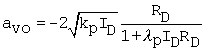
Finally, we can get an overall current dependence for av with the elimination of gm, using(4.5) with ![]() ≈ kp, which results in
≈ kp, which results in
Equation 5.6
Using an alternative form for gm (= 2ID/Veffp), also (4.5), the gain expression is
Equation 5.7
![]()
where
![]()
For simplicity, approximate forms of (4.5) and (4.13) of gm and gds are used here, which are independent of VSD. For reference, the “exact” and approximate forms of (4.5) and (4.13), respectively, are repeated here:
![]()
and
![]()
The “exact” equations of gm and gds are used in conjunction with the amplifier projects to compare the computed gain with the measured gain plotted against ID. This is done in both LabVIEW and Mathcad. Parameters kp and Vtpo (to get Veffp) will be extracted from the measured dc data, and λp will be used as an adjustable parameter to fit the SPICE and measured gain data.