
B.1. Fundamentals of Bipolar Junction Transistor Action
A bipolar junction transistor is made up of a sandwich of two semiconductor pn junctions. Transistors are either npn or pnp. In the active-mode transistor state, one junction, the input junction, is forward biased, and the opposite junction, the output junction, is reverse biased. The behavior of the individual pn junction diode will first be considered to clarify forward and reverse bias.
A semiconductor pn-junction diode in diagrammatic form is shown in Fig. B.1. The current and voltage of an ideal pn-junction diode are related by
Equation B.1
![]()
Figure B.1. Diagrammatic pn-junction diode. Applied voltage VD is shown for forward bias for which current freely flows. Opposite polarity is reverse bias, where the diode is essentially cut off and ID = –IS.
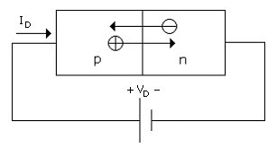
where VD is the voltage applied between the p and n regions (positive at the p terminal), ID is the responding current, and ISd is the saturation current. The thermal voltage, VT, is defined as VT = kT/q, where T is the temperature, k is the Boltzmann constant and q is the electron charge. At 27°C, VT ≈ 26 mV. VD is positive for forward bias and negative for reverse bias.
As illustrated by the arrows in the junction of Fig. B.1, for forward bias, the diode current consists of injection of holes from the p region (positive free carriers) into the n region and injection of electrons from the n region (negative free carriers) into the p region. The exponential factor in (B.1) is associated with the statistics of the free carriers, holes and electrons, and the effect on the lowering of the barrier to free-carrier flow of the application of the positive applied voltage.
The magnitude of ISd is dependent on semiconductor electronic properties such as doping levels and free-carrier lifetime and mobility. The magnitude of current flow for a given VD is dictated by a combination of the barrier-lowering factor (in the exponential) and the rate of free-carrier recombination; that is, carriers are annihilated by recombining with the opposite type of carrier on the opposite side of the junction from which they are injected.
A typical value for saturation current, ISd, is 10–11 mA, such that, for example, for VD = 0.6 V, ID ≈ 0.1 mA and increases by an order of magnitude for each additional increment of δVD ≈ 60 mV (at room temperature). The equation would suggest that for negative VD and |VD| >> VT, ID = –ISd and therefore is very small compared to the current under forward bias. In real pn-junction diodes, the current is larger and is not independent of the value of the reverse applied voltage. Nonetheless, it is still very small compared to the value of current for normal forward bias.
As mentioned above, the bipolar junction transistor is made up to two junctions, which share a common region. A pnp example is shown in Fig. B.2. The individual pn junctions of a transistor also exhibit diode characteristics, and the junction currents are related to the junction voltages by equations similar to (B.1). There is an essential difference that can be explained for the case of one junction being forward biased while the other junction is zero or reverse biased. Specifically, suppose that the transistor is a pnp (the other possibility being the npn) and the pn junction on the left (input junction) is forward biased and the pn junction on the right (output junction), is made to have zero bias by connecting a wire across this junction, as shown in Fig. B.2.
Figure B.2. Diagrammatic semiconductor pnp transistor. The input junction on the left has forward bias voltage VD, and the output junction on the right is shorted for zero bias. The input pn-junction diode current ID couples with the output pn junction to flow into the output p region.

Even though the forward-biased pn junction on the left shares the n region with another pn junction (on the right), it behaves like a pn-junction diode such that the current – voltage relation for the junction still has the form of (B.1) and is
Equation B.2
![]()
The saturation current is now designated IS, since IS ≠ ISd. [If the width of the n region is very large, the holes injected into the n region will recombine with electrons in the n region, and the associated current will flow entirely out through the contact to the n region. In this limiting case, the current – voltage relation for the junction on the left reverts to (B.1). The presence of the p region on the right will play no role.]
In a transistor, the n-region width is made small and the statistical chance of an injected hole surviving the transit across this region, without recombining with an electron, is very high. Upon entering the p region on the right, the holes are accommodated by the exit of an equal number of holes moving out at the contact to this p region. (Actually, they are converted to electrons at the interface of the contact and semiconductor to be consistent with having only electron flow in the metal contact and device connecting metal.)
In an ideal transistor, this is the only current mechanism. The various other current components of the real transistor are discussed below. These include electron injection that would be expected from the n region into the p region of the forward-biased junction on the left (as in Fig. B.2). In practice, special fabrication techniques are employed to make this component of current very small.
In the application of a transistor in the active mode, as for example, in an analog amplifier stage, the output junction is reverse biased, as shown in Fig. B.3. The junction configuration now represents a transistor; the regions are accordingly designated as emitter (E), base (B), and collector (C). Consistent with these assignments, the current into the transistor on the left is the emitter current, IE, and the output current on the right is the collector current, IC, and according to the mechanism described above for the ideal transistor, IC = IE.
Figure B.3. Diagrammatic semiconductor pnp transistor in active-mode operation. Regions are now designated emitter, base, and collector. The emitter – base junction is forward biased and the collector – base junction is reverse biased.

With forward bias (voltage) across the emitter – base junction and reverse bias across the collector – base junction, the emitter – base current equation, (B.2), is slightly altered, to become
Equation B.3
![]()
Variable subscripts have been changed to reflect the fact that the pnp structure is now specifically a transistor. (The parameter IS is the same in SPICE for the diode and the transistor models. ISd was used above for this discussion alone to differentiate between the two.) For reverse bias of the collector – base junction, the –1 of (B.2) is eliminated.
In this simplified version of the transistor, the output current is independent of the collector – base voltage. The possibility of infinite voltage gain is thus provided, because the output circuit behaves like a pure current source; that is, it will force current into an external resistance, which can be large without limit. This conclusion remains subject to additional alterations for the real transistor. However, in principle, the transistor mechanism as discussed is applicable short of certain limitations.
An example of obtaining gain from a transistor in an amplifier circuit is shown in Fig. B.4. A ground has been added at the n-region terminal to establish a reference. Therefore, the output voltage, VO, is defined with respect to this reference. To the transistor circuit of Fig. B.3, we have added an input signal Veb and a load resistor, RL. Note that since the input and output are referred to the base, the circuit is a common-base amplifier.
Figure B.4. Amplifier circuit incorporating a pnp transistor. The output voltage is with respect to ground at the n-region terminal. The base is common to the input and output and hence, this is the common-base amplifier configuration.
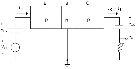
Suppose that initially, Veb = 0 and VEB is selected to give IC = 1 mA. This is, in an amplifier, the bias current. The output supply voltage is chosen to be VCC = 12 V. We select RL = 5 kΩ giving a bias output voltage VO = ICRL = 5 V. Note now that the collector-base bias voltage is VBC = VCC – VRL = 7V and the junction is reverse biased.
We now apply an input voltage (signal, ac, or incremental voltage) Veb = 18 mV. This increment added to VEB will cause IC to double (i.e., IC = 2 mA). The result is a new output voltage of vO(sig) = 10 V. Thus the incremental (or signal) output voltage is δVO = vO(sig) – VO = Vo = 5 V. Base – collector voltage is now vBC = VRL = 2 V and the junction remains in a reverse-bias state.
The incremental (ac or signal) ratio of output and input voltage is Vo/Vbe = 5V/18 mV = 278. Note that the gain is power-supply limited. Employment of a larger power supply permits the use of a larger RL, which results in a higher gain. We will later show that the gain is in fact VRL/VT based on an approximate linear representation between the input and output voltage. Note that in this case, the linear approximation is VRL/VT = 192, which indicates, for the example above, that the linear relation provides a fair estimate.
An alternative bias arrangement is shown in Fig. B.5. The input terminal is now that of the n region and the p terminal is a common node to the input and the output. This is the common-emitter configuration. Note that the voltage applied to the input junction has not changed, and the output junction now has a bias voltage of VEC – VEB and remains reverse biased as long as VEC>VEB.
Figure B.5. Common-emitter transistor amplifier configuration. The common terminal is now the p-emitter region and the input is at the base (n region). The output is between the common emitter and the collector. This diagram includes a possible IB and thus IC < IE, as is discussed in Unit B.3.

In electronic amplifiers, all three terminal configurations are possible: common base, common emitter, and common collector (emitter follower). Themost frequently employed amplifier stage is based on the common-emitter mode, but the other two serve important roles in electronic amplifiers. In all three, the emitter – base voltage is the input control-terminal voltage. In the common-emitter and common-base, the output current is the collector current and in the common collector, it is the emitter current. The common-collector configuration is usually referred to as the emitter follower.
In the subunits that follow, the detailed SPICE relations that generally relate the branch currents to the terminal voltages are developed. This includes the addition of many aspects of the real transistor which were not included in the discussion above of the highly idealized transistor.
Initially, the forward-active mode is explored, and this is followed by a discussion of the reverse-active mode. The reverse-active mode is where the situation in Fig. B.3 is reversed. Thus, VCB is positive (base – collector junction forward biased), while VEB is zero or negative. In the reverse-active mode, VCB becomes the input voltage, and the output current is the emitter current, IE.
Although the transistor is not operated in the reverse-active mode, the relationships developed for this case can be combined with those from the forward-active mode. The combination produces the general equations for relating currents and terminal voltages in transistors for all bias possibilities (i.e., where the transistor is biased out of the active mode).