
4.3. Transconductance Parameter
The transconductance parameter, gm, was introduced in Unit 2 in the treatment on the rudimentary electronic amplifier; it is the proportionality constant of the linear relationship between the output (responding) current and the input (control) voltage [(2.3)]. For the MOSFET, NMOS, or PMOS, Id = gmVgs, where Id is into the drain for both transistor types. An ideal transistor can be modeled with this alone. A simple model, which includes no other components, would often be adequate for making estimates of circuit performance.
To obtain an expression for gm as a function of the general form iD = f(vGS, vDS, vSB) [e.g., (3.8)], we use the definition [from (4.1)]
Equation 4.2

Using (3.8) to express iD, the resulting relation for gm is
Equation 4.3
![]()
where ![]() [(3.7)] and Veffn = VGS – Vtno. Note that the use of VDS is consistent with the partial derivative taken with respect to vGS, that is, Vds = 0. Also, the use of Vtno implies that vSB = 0. In general, VSB could be nonzero, although in the definition of gm, Vsb must be zero. For the case of nonzero VSB (bias), one substitutes for Vtno a constant Vtn(VSB) in the gm expression.
[(3.7)] and Veffn = VGS – Vtno. Note that the use of VDS is consistent with the partial derivative taken with respect to vGS, that is, Vds = 0. Also, the use of Vtno implies that vSB = 0. In general, VSB could be nonzero, although in the definition of gm, Vsb must be zero. For the case of nonzero VSB (bias), one substitutes for Vtno a constant Vtn(VSB) in the gm expression.
Alternative forms for the gm expression can be obtained from (3.8), which is, solving for Veffn,
Equation 4.4
![]()
Using (3.8), (4.3), and (4.4), gm takes on altogether three forms:
Equation 4.5
![]()
Usually, in initial design, kn replaces ![]() to eliminate the VDS dependence without a serious penalty in accuracy.
to eliminate the VDS dependence without a serious penalty in accuracy.
Using the simple linear transistor model, an expression for the circuit transconductance, Gm, for the circuit of Fig. 4.1 will now be obtained. The input loop equation for an applied gate signal voltage, Vg, is
Equation 4.6
![]()
which is, with Vgs = Id/gm,
Equation 4.7
![]()
and
Equation 4.8
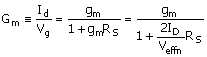
The far right-hand side uses (4.5). For example, for a 1-V drop across RS and Veffn = 0.5 V, Gm = gm/5. Note that the ratio of the signal voltage drop across RS and signal voltage Vgs is gmRS:1. The Gm concept is utilized routinely in MOSFET circuits (and BJT circuits), which gives the effective reduced transconductance, referred to Vg, in the presence of the source resistor.