C.6. Selection of Coupling Capacitors
External capacitors are added to the circuits of this unit for two purposes. One, shown in Fig. C.1(b), is to connect the signal input source to the amplifier. The other is a special-purpose capacitor of the amplifier project. It is attached to facilitate measurement of the base – emitter voltage with high resolution. Design considerations for selection of the capacitor values are discussed in the following.
C.6.1. Coupling Capacitor for the Common-Emitter Amplifier
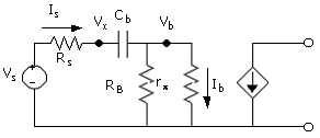
The linear equivalent circuit of the amplifier of Fig. C.1(b) is shown in Fig. C.6. The selection of the value of the capacitor Cb is based on the requirement that it has negligible effect on the signal current at any frequency at which the amplifier will be operated. Including the reactance of the capacitor, the input signal current is
Equation C.29

Figure C.6. Signal model of the circuit for the determination the characteristic frequency of the frequency response associated with the coupling capacitor.
The input signal current magnitude is
Equation C.30

where
Equation C.31
![]()
Frequency f3dB is defined as the frequency where the response magnitude is
Equation C.32
![]()
It follows that for this case, f3dB = fb. Note that at f = 10f3dB,
![]()
C.6.2. Coupling Capacitor for Measuring the Base Input Voltage
In Project C1 measurement of the base input voltage is made at the signal side of the coupling capacitor. This is the node designated by Vx in Fig. C.6. Good measurement precision is provided, as the dc component of the base voltage is blocked by the coupling capacitor. The maximum voltage sensed by the input channel is only the signal voltage Vb ≈ Vx ≈ 5 mV, as discussed in Unit C.4. This value is much smaller than dc VBE ≈ 0.5 V. In this configuration, the limit setting for the input channel is set at 0.1 V, for a resolution of about 48 μV with the input channel in the bipolar mode. If the peak signal voltage is, for example 5 mV, the resolution is about 1% of the measured voltage
The required capacitor, Cb, for this case and for same f3dB, is substantially larger than that obtained from (C.31). As will be shown, at f ≈ f3dB, the requirement is that |XCb| ≈ rπ. It follows that at f near f3dB, Rs >> |XCb| since Rs >> Rb ≈ rπ. The input signal current is thus given approximately by
Equation C.33
![]()
This includes the good assumption that Rs >> Rb and that, by design, |XCb| ≈ Rb for f ≈ f3dB. (Technically, the pole of the transfer function is ignored.)
The signal voltage, Vx(f), at the input signal source side of the capacitor is the sum of the voltage at the base plus the voltage across the capacitor, that is, with (C.33),
Equation C.34
![]()
The ratio Vx(f)/Vb is thus
Equation C.35
![]()
Note that the form of Vx(f) is falling, for increasing frequencies, to a plateau (Vb). We will define f3dB as the frequency where the magnitude of this ratio is ![]() . This could qualify as a type of corner frequency, as it represents the frequency where the frequency response function is
. This could qualify as a type of corner frequency, as it represents the frequency where the frequency response function is ![]() times the asymptotic value. A solution for f3dB then comes from
times the asymptotic value. A solution for f3dB then comes from
Equation C.36

giving
Equation C.37
![]()
At f=10f3dB, Vx = 1.005Vb. Note that for this case of a current source [(C.33)], the value of the capacitor can be obtained simply to satisfy |XCb| = rπ.
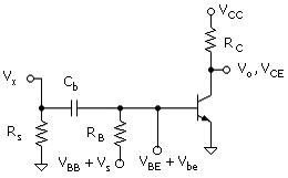
C.6.3. Coupling Capacitor for the Base Voltage Measurement of the DC Sweep Circuit
The project circuit for making a precision measurement of the gain of the amplifier of Fig. C.1(a) is shown in Fig. C.7. The circuit has the addition of Cb and Rs for measuring the base signal voltage without the dc component. The selection of Rs in the amplifier project is made to satisfy if Rs >> rπ such that the effect on the gain referred to Vs is small. The choice is, on the other side, Rs < RB, such that the charging time of Cb is not prohibitively long during the bias sweeps. The f3dB frequency at Vx for this case is (C.31) with fb = f3dB. In the amplifier project, the capacitor is selected from (C.37) to satisfy the requirement for the amplifier of Fig. C.1(b) using (C.37). The capacitor will thus certainly be adequate for the amplifier of Figs. C.1(a) and C.7.
Figure C.7. Common-emitter amplifier for measuring the amplifier gain as a function of bias current. The signal base – emitter voltage is measured at Vx.