
Hardware and Software Requirements
Circuit connections to the DAQ require a cable and a facility for connecting to individual pins. An efficient system is based on a National Instruments Connector Block (CB-68LP) and a basic circuit board as shown here.

Connections to the circuit board from the connector block are made one time. The two resistors of the circuit are connected to output channels 0 and 1, respecively. Thus, for example, Chan0_out, as noted, is dedicated to the top strip on the circuit board. The bottom top strip is associated with Chan0_in, and so forth.
All of the project LabVIEW files are programmed to be consistent with the plus bus (rail), Chan0_out, and the minus bus (rail), Chan1_out. Therefore, it is intuitively helpful to have the output channels physically connected in this fashion.
The project examples included with the book were conducted on a special circuit box that connects directly to the shielded 68-pin connector. This bypasses the connector block. A shielded cable is strongly recommended in any event. Many of the projects involve the measurement of relatively low voltage signals.
In addition, the lab projects included in the book require the following (or equivalent):
Pentium PC (or equivalent).
National Instruments DAQ PCI-MIO-16E-4.
LabVIEW 6.0i Student Edition or LabVIEW 6.0i or later version.
Mathcad Professional 2001 or later version.
National Instruments Shielded 68-pin Cable.
|
Semiconductor Devices and Components (Recommended) 6-Transistor (3-gate) CMOS Array – CD4007[*] CMOS Opamp – SGS-Thomson TS271[**] NPN - Medium-Power NPN BJT – NTE186[***] PNP - Medium-Power PNP BJT – NTE187[****] Capacitors Resistors
| ||||||||||||||||||||||||||||||


[*] The CD4007 chip contains three CMOS inverters or three PMOS and three NMOS transistors. Since they are inverters, NMOS and PMOS pairs have Hardware and Software Requirements internally connected gates. However, this does not prevent having a sufficient number of the individual transistors in the analog laboratory projects.
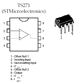
[**] The TS271 is chosen as it has simple external resistor biasing. Thus, students can gain an intuitive feel for the relation between the characteristics of the CMOS opamp and bias current with straightforward exchange of bias resistors. In the case of a group of students, for example, each student can select a different bias current, such that all of the results can be assembled to plot the opamp characteristics, such as gain and frequency response versus bias current. In addition, the circuitry of the opamp is straightforward and may be understood within the scope of the book. Extensive experience in our laboratory with devices has demonstrated that this opamp can withstand considerable abuse without failing even though it is a MOSFET chip. It is however, strongly advised that the power supply never be turned on until the power-supply pins, input pins and output pin are connected in the circuit.
[***] The NTE186 is a rugged npn BJT that is investigated at current levels well below the normal operating range. Heating of the device is thus minimized and for the measurements, it can be assumed to be at room temperature. Also, various high-level injection effects, which render the basic SPICE parameter set invalid, are avoided.
[****] Complementary paired with the NTE186.