
C.7. Common-Emitter Amplifier with Active Load
In the early days of electronic amplifiers, the voltage amplification device was, of course, the vacuum tube. It existed in only one polarity configuration, that is, with positive plate (bus or rail) voltage. With the appearance of semiconductor transistors came the availability of the dual set of devices with opposite terminal voltage polarities. This is the case for BJTs, JFETs, and MOSFETs. (Vacuum tubes were implemented in class B amplifiers. The application required a pair of inputs, one 180° out of phase with the other, normally derived from a transformer.)
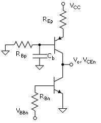
The dual set has provided the versatility for a wide range of electronic system applications, including the amplifier with active load shown in Fig. C.8. This can be compared with the circuit of Fig. C.1, which in place of the pnp transistor, has a bias collector resistor, RC.
Figure C.8. Common-emitter amplifier with active (transistor) load. The npn is the driver transistor and the pnp is the load transistor. The input signal source could be moved to the base of the pnp, in which case the two transistors play opposite rolls.

Note that either transistor base could serve as the input such that the opposite transistor becomes the load. In Fig. C.8, the npn is chosen as the driver transistor and the pnp as the load transistor.
A dc output characteristic plot is shown in Fig. C.9. Since the collector current of the individual transistors is the same, the solution to bias voltage VCE for the npn is the intersection of the two curves, that is, 5 V. This would be a good choice for a bias output voltage for the power supply voltage of this case, which is 10 V. For the plots, VAFn = 100 V and VAFp = 20 V were used. (In the discussion of the npn – pnp amplifier, the added subscript n or p will denote npn or pnp, respectively.)
Figure C.9. Output characteristics for the npn and pnp transistors. The pnp emitter – collector voltage is vEC = VCC – vCE, where vCE is the collector – emitter voltage of the npn. The bias variables VCE, VEC, and IC are at the intersection of the two plots.

A signal impressed at the base of the npn causes the npn curve to move up or down while the pnp curve remains in place. Note that the pnp acts like a load line of a resistive load; however, an extension of the active-region characteristic of the pnp intersects the zero-current axis at VCC + VAFp = 30 V. The pnp active-load transistor thus provides the equivalent of a bias resistor with a power supply of 30 V instead of the actual 10 V.
C.7.1. Gain of the NPN – PNP Common-Emitter Amplifier with Active Load
The gain benefit for the case of the active load is apparent from the following. The equation for the gain of the BJT common-emitter amplifier with resistor RC, which includes the output resistance of the driver transistor (in this case, npn), is a form of (C.28)
Equation C.38
where ron is the output resistance of the npn and is given by [generalization of (C.13)]
Equation C.39
![]()
where VCE and VBE are the transistor bias voltage variables and IC is the collect bias current of the amplifier. Parameters VAFn and VAFp are used in this unit for the slope parameter for the npn and pnp, respectively.
The output resistance expression is generalized here to emphasize that strictly speaking, the collector currents and voltages must match as suggested in the expression. Voltages VBE and VCE are bias values. In the following, as is standard in electronics circuit analysis, we approximate the output resistance, for example, for the npn as follows:
Equation C.40
![]()
It follows that for the pnp
Equation C.41
![]()
where IC ≡ IC(VCE), that is, the actual bias collector current.
For the pnp active load, the resistor RC is now replaced with the output resistance of the pnp, to obtain
Equation C.42
![]()
where the far right-hand side uses gm = IC/VT.
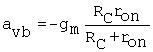
The gains for the resistive load and active load cases can readily be compared with the substitution of gm = IC/VT in (C.38) (gain with load RC) and (C.40) for ron to obtain
Equation C.43

For the example of VCC = 10 V and bias VCE = 5 V, VRc = 5 V. Using VAFn = 100 V and VAFp = 20 V, the room-temperature gain magnitudes are |avbRc| = 4.76 V/0.026 V=183 for the amplifier with Rc load compared to an npn – pnp amplifier gain magnitude of |avb| = 16.7 V/0.026 V=641. In practice, the advantage will be considerably more, as the value for VAFp used here is smaller than normal for BJTs. The small number was used above in the plot (Fig. C.9) to exaggerate the effect of the slope.
C.7.2. Output Resistance at the Collector with an Emitter Resistor
In Project C2 the effect of an emitter resistor in the emitter branch of the pnp, REp, on the output resistance of the pnp will be explored. The circuit is shown in Fig. C.10. The effect of the emitter resistor is to increase the output resistance, due to the negative feedback effect, at the collector of the pnp. This increase can be made to be substantial; in fact, to a good approximation, the load on the amplifier is only ron of the npn.
Figure C.10. Amplifier with an emitter resistor in emitter branch of pnp to increase the output resistance at the collector of the pnp. Also included is a capacitor, Cb, for grounding (signal) the base voltage of the pnp.
The generalized gain expression, which includes the effect of the emitter resistor, is
Equation C.44
![]()
where Rop is the output resistance at the collector of pnp, for the circuit with REp.
Here, we develop an expression for the output resistance of a BJT with the emitter resistor. This is a function of both REp and RBp. In the Project C2 the amplifier gain is measured with and without a base shunt capacitor, Cb. With the capacitor in place, the base resistance in the signal circuit is effectively zero, and this alters Rop significantly. The linear circuit for the general case of a BJT common-emitter amplifier with emitter resistor is shown in Fig. C.11. The circuit includes a base resistor, RB.
Figure C.11. Linear circuit for the determination of the output resistance at the collector for a circuit with emitter and base resistor.
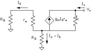
A test voltage, Vo, is applied at the collector with the base resistor and emitter resistor at signal ground. In response, a current Io flows from Vo through RE in parallel with RB + rπ. This induces a voltage VRE = (Io – Ib)RE across RE that is applied to rπ in series with RB. Base current Ib is a fraction of Io as given by
Equation C.45

Applied voltage Vo sums up to
Equation C.46
![]()
The approximation is based on ro >> RE and is consistent with the fact that the signal voltage drop across the output of the transistor is much greater than across the emitter resistor.
Eliminating Ib in (C.46) using (C.45) results in the solution for Ro, which is
Equation C.47
![]()
The result has two limiting forms based on the relative value of RB: When RB >> rπ + RE,
Equation C.48

The approximate form uses IC ≈ IE.
Intuitively, for RB → ∞, the feedback current, gmIbrπ, goes to zero.
For RB→0,
Equation C.49

The alternative forms on the right in (C.48) and (C.49) use (C.15), βac = gmrπ. Again, the approximate form uses IC ≈ IE. Note that the solution corresponds to the maximum fraction of Io that can flow through rπ(RB = 0), to induce a feedback current.
When applied specifically to the npn – pnp circuit of Fig. C.10, the limiting case is, for RBp zero,
Equation C.50
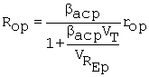
where Rop is the signal resistance looking up into the collector of the pnp. For example, if REp is selected to produce VREp = 1 V and βacp = 50, the denominator is roughly 2, such that Rop ≈ (βacp/2)rop. In this case, the load on the amplifier is due almost entirely to the output resistance looking into the collector of the npn (Ron = ron), with the result that the gain is [from C.44]
Equation C.51
![]()
The other extreme is for RBp >> rπp + REp, where Rop ≈ rop [(C.48)]. The gain reverts to (C.42), repeated here
![]()
The npn – pnp amplifier circuit of Fig. C.10 is used in the project on the amplifier to investigate the signal-derived magnitude of the slope parameters of npn and pnp transistors. Using a bypass capacitor at the base of the npn, as discussed below, the signal circuit will effectively have RB = 0, and a gain measurement along with (C.51) yields VAFn. The gain will also be measured for the circuit without the capacitor and with RBp >> rπp + REp (by design). For this case, (C.42) applies and the gain measurement provides information on the combination output resistance parameter, VAFnp. Between the two measurements, values for both parameters are determined.
In the measurement circuit of the npn – pnp amplifier, the gain referred to the signal source (amplifier circuit gain) is
Equation C.52
![]()
where Ronp is the signal resistance at the output node (Fig. C.10), that is, the combined resistance looking back into the collects of the npn and pnp transistors. In general, this is
Equation C.53
![]()
With RBp effectively made zero with the shunting capacitor, Ronp ≈ ron = VAFn/IC. Without the capacitor, Rop is obtainable from (C.47) for use in (C.53).
In the amplifier project, the circuit-gain equation (C.52) is used to convert measured gain into Ronp and then information on VAFn and VAFp. With the availability of these numbers, we can then calculate the gain produced by the transistor (base to collector), using (C.44).
C.7.3. DC (Bias) of the NPN – PNP Amplifier
The circuit equations for the circuit of Fig. C.10 are (collector power supply through pnp base)
Equation C.54
![]()
and (npn base)
Equation C.55
![]()
In the project on the amplifier, RBp is determined for a design collector current. The selection uses (C.54) with, for example, VCC ≈ 9 V, that is, less than the maximum available from the DAQ output. Then with RBn = RBp, VBBn will be less than VCC by the amount of the drop across REp (for example, 1 V). This makes the good assumption that βDCn ≈ βDCp, A LabVIEW program then sets up the circuit for the design collector current by adjusting two supply voltages (DAQ output channels).