
13.4. Common-Source Stage as a Series – Series Feedback Circuit
The circuit of Fig. 13.2 with the source resistor is technically a feedback circuit. It falls into the category of series – series feedback, or the feedback network samples the output current and feeds back a voltage in series (and the same polarity, negative feedback) with the input to the common-source stage, that is, Vgs3. The series – series feedback amplifier is referred to as a transconductance amplifier. The noninverting and inverting opamp configurations are series – shunt (voltage amplifier) and shunt – shunt (transresistance amplifier), respectively. An additional alternative is shunt – series (current amplifier). An example of this type of feedback amplifier is discussed in Unit 13.5.
In Unit 9.9, an expression for the output resistance of the current source (drain current) with source degeneration was obtained [(9.9)]. This is
![]()
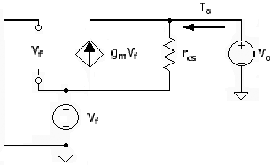
The perspective of the common-source amplifier in a series – series feedback mode is shown in Fig. 13.3. The circuit configuration is for determining the output resistance. A voltage Vo is applied at the output terminals with the input grounded. In this series – series circuit, a feedback voltage, Vf, which is proportional to the current Io, is induced as indicated in the circuit diagram. With the input grounded, voltage Vf is applied to the input terminals of the transistor. The loop equation at the output is then
Equation 13.7
![]()
Figure 13.3. Linear circuit for deriving the output resistance for the series – series feedback circuit. The feedback voltage is proportional to the output current.
By comparison of the feedback circuit of Fig. 13.3 with the circuit of Fig. 13.2, Vf = IoRS3. Thus,
Equation 13.8
![]()
This produces (9.9) from Ro = Vo/Io and with rds = 1/gds. Intuitively, the feedback is such as to cause a much larger current through rds than Io, and therefore a much larger Vo is required for a given Io.
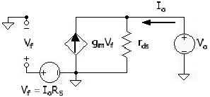
Dropping the RS as in the right-hand side of (13.8) renders the result equivalent to the ideal series – series feedback amplifier, as shown in Fig. 13.4. In the ideal series – series amplifier, the sense function has zero resistance; that is, the output voltage is directly across rds. With gm/gds >> 1, the ideal circuit provides a very good approximation to the actual circuit. For example, with Veffn = 0.5 V and λn = 1/50 V, the ratio is 100.
Figure 13.4. An ideal series – series feedback amplifier. Vo is applied directly across the output resistance and Vf is applied to the grounded input.
For both feedback amplifier types with series as the second term (series – series and shunt – series), the output resistance is increased by a factor (1 + T), where T is the loop gain, as in the discussion of the opamp feedback amplifiers in Unit 11. The loop gain for the common-source circuit of Fig. 13.2 is, by definition, T = Vf/Vgs3. By inspection of (9.9) we conclude that T = gm3RS3. In terms of T, the output resistance is then
Equation 13.9
![]()