
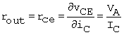
2.4. Transistor Output Resistance and Limiting Gain
The linear-equivalent circuit of Fig. 2.2 includes an idealization in that the output is a pure current source. In real transistors, the collector (BJT) or drain (MOSFET) current increases with increasing VCE or VDS. This is accounted for by including an output resistance, rout, in the linear model, as added to the circuit in Fig. 2.5. For the BJT and MOSFET, respectively, the value of rout is
Equation 2.9
Equation 2.10
![]()
Figure 2.5. Basic linear circuit with transistor linear model. Circuit includes signal source voltage and load RL, Transistor model now includes output resistance rout.

where VA is the characterizing transistor parameter. Note that this voltage dependence is not included in (2.1) and (2.2); these equations are consistent with the simplified circuit model of Fig. 2.2. Similarly, the voltage dependence will alter gm from the simple forms of (2.4) and (2.5). This is discussed in Unit 4.
The actual gain, with a load RL, which includes the output resistance, can be obtained from modification of (2.7) to include rout in parallel with RL as in Fig. 2.5. The result is
Equation 2.11
![]()
The parameter VA of both transistors can typically be about 100 V. (In MOSFETs, the parameter is usually referred to as λ, which is the reciprocal, λ = 1/VA.) A useful comparison between the devices is the maximum limiting gain of the common-emitter and common-source amplifier voltage gains, which applies for the case of RL → ∞. The gain in this case is
Equation 2.12
![]()
Using (2.4), (2.5), (2.9), and (2.10), we obtain for the limiting gain:
Equation 2.13

Equation 2.14
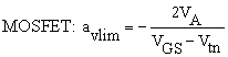
Using sample numbers from above, the comparison gives av lim(BJT) ≈ –4000 and av lim(MOSFET) ≈ –400. The vacuum tube, type 6SN7, has a typical output resistance rout ≡ rp ≈ 7KΩ (p for plate), which leads to a limiting gain magnitude of about 21. (This is referred to as the μ of the tube.) You have to respect the amplifier designers of the vacuum-tube era when considering what was accomplished despite the limitations of these amplifying devices.
In modern integrated circuits, it is possible to implement load circuits, which have an effective RL >> rout such that the limiting gain can be achieved. This is particularly important in MOSFET amplifiers to make up for the relatively low value of gm.