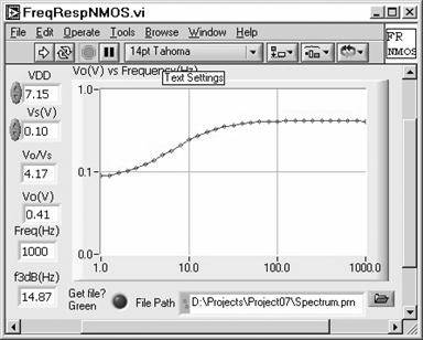
In FreqRespNMOS.vi, the frequency of the with source voltage (sine-wave Chan1_out) is swept from 1 to 1000 Hz. Chan2_in should be disconnected to reduce the stray capacitance at the gate. In the Front Panel of the VI, set VDDbias and Vs at the values determined in the gain measurement with GainNMOS.vi.
Along with FreqRespNMOS.vi, open FG1Chan.vi to observe the output waveform. Verify that Cs is installed and run the VI to obtain a value for f3dB.
Open, from the Diagram of FreqRespNMOS.vi, Frame 2, XYtoDataFile2.vi. Run FreqRespNMOS.vi again, with the data mode switch set to Green (logic stage 1), to obtain a data file of the frequency-response plot in XYtoDataFile2.vi. (Note that with the data VI open, the data are transferred to the VI and can then be saved in the VI.) The data file is used in the Mathcad project file. Default and save the Front Panels of both XYtoDataFile2.vi and FreqRespNMOS.vi. Note the maximum index for the Mathcad file. The f3dB result will differ from the design, as the design was based on the simple form. This will be explored in the Mathcad file.
A data file can be obtained later from the saved data in the graph of FreqRespNMOS.vi, with XYtoDataFile2.vi. As noted above, the data file VI can be obtained from the Diagram of FreqRespNMOS.vi. The data file VI is located in Dat.llb in the User.lib folder (Program Files>>National Instruments>>LabVIEW 6). The VI can also be accessed from the menu sequence in FreqRespNMOS.vi, Browse>>Show VI Hierarchy, and open the data file VI from the Hierarchy Window.