
5.4. Current-Source Common-Source Amplifier: Common-Source Amplifier with a Source Resistor
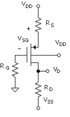
The bias circuit of the current-source bias amplifier, shown in Fig. 5.6, has a dual power supply. One advantage of this is that the input is at zero dc volts such that the signal can be connected directly without interfering with the bias. The dc circuit equation for setting up the bias is
Equation 5.14
![]()
where ![]() .
.
This circuit is more bias stable than the grounded source amplifier, as slight changes in VSG (due to device parameter variations or temperature) are usually small compared to VDD. Note that Vtp is used in lieu of Vtpo as VBS ≠ 0. The chip (CD4007) used in the projects is a p-well device (as noted in Unit 3), with the NMOS transistors in the well. The well is connected to VSS, while the body of the chip is connected, as in Fig. 5.6, to VDD. The pn junction formed by the well and the bulk is thus reverse-biased with a voltage |VSS| + VDD.
Figure 5.6. Dc circuit of the dual-power-supply common-source amplifier. The gate is at ground potential, allowing the signal to be connected directly to the gate. RG is necessary only to prevent shorting out the input signal.
In the amplifier projects, however, we have the latitude to connect the body and source as there is only one transistor in the circuit and the body can float along with the source. Thus we can assume that Vtp = Vtpo. As shown in Fig. 5.7, the signal circuit requires the addition of a bypass capacitor, Cs. This places the source at signal ground provided that the capacitor is large enough. The criterion for this is discussed in Unit 6. The voltage-gain equation is the same as in the amplifier, with the source actually grounded.
Figure 5.7. Amplifier circuit with a bypass capacitor attached between the source and ground to tie the source to signal ground. Signal input is attached directly to the gate. Body and source are connected internally in the project chip for the transistor used in the amplifier.

Without the bypass capacitor, RS is in the signal circuit and a fraction of the applied signal voltage at the gate is dropped across the resistor. The signal circuit for this case is shown in Fig. 5.8. The circuit transconductance of the amplifier with RS was discussed initially in Unit 4. This is reviewed in the following.
An applied input signal, Vi = Vg, divides between the gate – source terminals and the source resistor according to [(4.6)]
Vg = Vgs + IdRs
Figure 5.8. Signal circuit for dual-power supply common-source amplifier. Input signal voltage, Vi, is divided between Vgs, the control voltage, and the source resistor according to the ratio 1: gmRS.

When combing this with Id = gmVgs, we obtain [(4.7)]
![]()
The circuit transconductance, Gm, is then [(4.8)]
![]()
The gain for this case is thus (neglecting gds)
Equation 5.15
![]()
In one of the amplifier projects, RS = RD, and the gain without the bypass capacitor is actually less than unity.