
C.2. Linear or Signal Model for the BJT
The primary function of a transistor in analog circuits is to produce a signal output current in response to a signal input voltage. In the case of the common-emitter circuits of Fig. C.1, the transistor input voltage is Vbe and the responding output current is the collector current Ic. (Variable subscript conventions are covered in Unit 2. Uppercase symbols with lowercase subscripts denote RMS or peak magnitude of periodic signals.) The linear relation between the two variables is the transconductance, gm. By definition, for the BJT
Equation C.7
![]()
In some simple amplifier circuits, this would be all that would have to be known about the transistor to perform a design or analysis. More generally, however, the model also includes input and output resistances, ri = rb + rπ and ro, respectively. The transistor linear model, which includes these components and a load resistor (in this case, bias resistor, RC), is shown in Fig. C.2. Applied input voltage Vbe and responding Ic are indicated.
Figure C.2. Linear signal model for the BJT. Model parameters are rb, rπ, gm, and ro. Added to the model are circuit components RC and applied voltage Vbe.

The input resistance relates the input signal base current Ib to the signal emitter – base voltage, Vbe, that is
Equation C.8
![]()
Parameter rb is the actual physical resistance through which the base current must flow to arrive at the true, internal physical base – emitter junction. The signal voltage across the internal base – emitter junction is ![]() . Parameter rπ is the linear relation between Ib and
. Parameter rπ is the linear relation between Ib and ![]() and is not a physical resistance.
and is not a physical resistance.
We assume in the following discussion that rπ >> rb. This is especially true in the low current range of our BJT transistor projects. As will be seen below, rπ is inversely proportional to bias collector current, IC, whereas rb is close to a constant and could be significant at currents corresponding to midrange or higher for the transistor. (As a rule, rb must be taken into consideration when the model is applied in very high frequency applications.) Note that neglecting rb compared to rπ is equivalent to ![]() , as assumed below.
, as assumed below.
The output-resistance parameter, ro, accounts for the fact that total collector current, iC, increases with increasing total collector – emitter voltage, vCE. According to the output resistance parameter relationship, the current through this resistance is
Equation C.9
![]()
Including ro, the current through the load, in this case bias resistor, RC, is
Equation C.10
![]()
This current flows up through RC such that Vce is negative for positive Vbe. Thus, the current associated with ro subtracts from gmVbe to reduce the current through RC. For a positive Vbe, there is an increase in the total vBE, thus causing the total collector current to increase. The result is a decrease in the total vCE and hence a negative incremental Vce.
The two components of (C.10) are illustrated graphically in Fig. C.3. The output characteristics are for two values of base – emitter voltage: bias only, VBE, and bias plus base – emitter signal voltage, VBE + Vbe. They are designated Bias and Signal. The solution to iC and vCE is constrained to the “load line,” which is iRc = iC = VCC/RC – vCE/RC [(C.5)].
Figure C.3. Transistor output characteristic with no signal and signal. Also plotted is the RC load line. The solution for iC and vCE is always the intersection.

At a constant vCE = VCE, the change in the current-source current for the applied Vbe is gmVbe [(C.7)]. The net collector current change (signal current), Ic, though, is as given by (C.10); that is, it includes the component associated with ro. Since the output characteristic slopes downward for decreasing vCE, the actual transconductance decreases, but the linear model treats this effect with a constant gm combined with the effect of the output resistance, ro.
C.2.1. Determination of the Linear Model Parameters
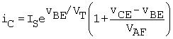
We can relate the values of the two parameters in (C.10) to the SPICE model parameters using (B.7) with the substitution vBC = –(vCE – vBE). This is
Equation C.11
Differentiating (C.11) with respect to vBE (with vCE = VCE, Vce = 0), gm is found to be
Equation C.12

The approximate form only ignores a term on the order of IC/VAF, where VAF >> VT.
The output resistance is obtained with vBE = VBE (bias value) or Vbe = 0. This is
Equation C.13
![]()
where, from (C.11), IC(vCE = VBE) = ISexp(VBE/VT). For simplicity, the bias collector current, from (C.11), IC = iC(VCE), is usually used for the calculation for ro. Finally, a relation for rπ comes directly from (C.7), Ic = gmVbe, and (B.41), Ic = βacIb. Equating the two gives
Equation C.14
![]()
Hence, from the definition rπ = Vbe/Ib (with ![]() )
)
Equation C.15
![]()
Note that the right-hand side of (C.14) is the alternative current-dependent current source of the linear model of Fig. C.2.
As discussed in Unit B.9, βac can be slightly different from βDC, but the distinction usually need not be made in analysis or design. This is due to the fact that βDC tends to be quite variable among devices and that most analog designs are based on making the results as independent of βDC as possible. Signal parameter βac will be used in the following, but it is understood that βDC can be used in the calculations without serious penalty in precision.