As will be explored in a project Mathcad file, the basis stability computation is performed here with LabVIEW. Recall (Section 5.5) that this takes into consideration a possible range of Vtno and kn values. Here, an analysis is made regarding the extent to which your design is optimum in terms of bias stability. Note that this is separate from the maximum signal condition that has been included in the design.
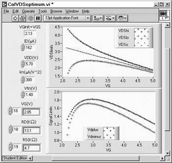
Open CalVDSoptimum.vi. In the Digital Controls, set you values for VDD, kn, Vtno, and ID. ID is the nominal value of the design for the nominal values of the parameters. Your value of ID, along with your parameter values, will be assumed to be, for this evaluation, the nominal values. The computation holds the bias current constant at the design value (as entered into the Front Panel). As VG is increased (X axis), the added increment of VG is the added drop across the new RS, for a given new VG. Run the VI.
Verify that the value of VGS in the top Digital Indicator matches reasonably well your measured value (Front Panel of GainNMOS.vi). This SPICE computation uses your measured parameter values and ID. The values should be consistent.
The top graph is its VDSlimits versus VG. The center (dashed) curve is for your parameters. The downward slope reflects the increasing drop across VG. The top and bottom plots are for the two extremes of VDS that occur for the worst case of the combination of the limits of kn and Vtno. The computation is for Vtno± = Vtno ±100 mV and . The same optimum signal level condition as used in your design is maintained throughout.
The lower graph contains plots of the output signal limiting values. The best combination of bias stability and signal level is at the peak of these curves.
Step through the RS Array Digital Indicator to locate your RS and the associated index. Then determine the corresponding VG and RD (same index). The value of RD should match your design value. The value of VG should match the value from the Front Panel of GainNMOS.vi.
Locate your value of VG on the X-axis of the two graphs. If it falls in the range of values surrounding the peaks, the circuit is optimized both in terms of signal limits and bias stability. Note that bias stability was not taken into consideration in the design. In the design, though, often a given criterion serves as the basis and the design may then be evaluated for other criteria.