
Instruction Set Changes
Introduction
The Fast System Call/Return instruction pair was added in the Pentium® II processor:
A detailed description can be found in “Fast System Call/Return Instruction Pair” on page 708.
Support for the new instructions is indicated in the capability bit mask returned in the EDX register (bit 11) on executing a type 1 CPUID request (see Figure 28-1 on page 708).

Fast System Call/Return Instruction Pair
Background
Normally, when an application program (i.e., a program that is executing at privilege level 3) calls the OS, the processor incurs a significant amount of overhead in performing the privilege level checks necessary to ensure that the caller is permitted to call the target privilege level 0 code.
The Pentium® II added a new facility referred to as Fast System Call. It consists of the following elements:
The SYSENTER instruction.
The SYSEXIT instruction.
Three new MSRs (SYSENTER_CS_MSR, SYSENTER_ESP_MSR and SYSENTER_EIP_MSR).
The Fast System Call facility permits a fast call to a procedure in the OS kernel and a fast return to the calling program.
The OS Initialization of the Fast Call Facility
The OS sets up the three MSRs to define the entry point of the OS procedure that can be called by privilege level 3 programs using the SYSENTER instruction and a Stack area to be used by the OS procedure when it is called.
The OS Creates Four GDT Entries
Before setting up the three MSRs, the OS sets up the following 8-byte segment descriptors in the GDT in the order specified (they must occupy sequential GDT entries):
An 8-byte Code Segment descriptor in the GDT that defines the code segment that the target OS procedure resides in. The descriptor must define the code segment as having the following characteristics:
- Flat Model.
- 32-bit code segment.
- Up to 4GB in size.
- Execute-only.
- Read-only.
- Accessed.
- Non-conforming.
The next 8-byte entry in the GDT defines the Stack Segment that the OS procedure will use when it is called. The descriptor must define the Stack segment as having the following characteristics:
- Flat Model.
- 32-bit stack segment.
- Up to 4 GB in size.
- Read-Writable.
- Accessed.
- Expand Up Stack.
The next 8-byte entry in the GDT defines the code segment that the calling privilege level 3 program resides in. The descriptor must define the code segment as having the following characteristics:
- Flat Model.
- 32-bit code segment.
- Up to 4GB in size.
- Execute-only.
- Read-only.
- Accessed.
- Non-conforming.
The next 8-byte entry in the GDT defines the Stack Segment for the calling program that will be returned to upon execution of the SYSEXIT instruction in the OS procedure. The descriptor must define the Stack segment as having the following characteristics:
- Flat Model.
- 32-bit stack segment.
- Up to 4 GB in size.
- Read-Writable.
- Accessed.
- Expand-Up Stack.
The OS Sets Up the Three MSRs
Having set up these four descriptors in the GDT, the OS then sets up the three MSRs as follows:
- The SYSENTER_CS_MSR is loaded with the 16-bit selector that will select the first of the four descriptors in the GDT.
- The SYSENTER_EIP_MSR is loaded with the 32-bit offset that points to the entry point of the OS kernel procedure to be called.
- The SYSENTER_ESP_MSR is loaded with the 32-bit offset of the Top-of-Stack to be used by the OS kernel procedure when it is called.
This completes the initialization that must be performed by the OS before the Fast Call facility can be used by privilege level 3 programs.
The following two sections provide a detailed description of the SYSENTER and SYSEXIT instructions.
The SYSENTER Instruction
When the SYSENTER instruction is executed, the processor takes the following actions:
It loads the 16-bit segment selector from the SYSENTER_CS_MSR into the CS register. This causes the processor to read the first of the four descriptors from the GDT. This defines the start address and length of the Code Segment that contains the OS procedure to be called.
It loads the instruction pointer from the SYSENTER_EIP_MSR into the EIP register. At this point, CS:EIP points to the entry point of the OS kernel procedure to be called.
The SS register is loaded with a GDT selector value that selects the second of the four descriptors in the GDT. This descriptor describes the Stack Segment to be used by the OS procedure when it is called. This descriptor is read from memory, giving the processor the description of this stack segment.
It loads the stack pointer from the SYSENTER_ESP_MSR into the ESP register. At this point, SS:ESP points to the top of the stack to be used by the OS procedure when it is called.
The processor switches to privilege level 0.
If the calling program is a VM86 task, the processors clears EFlags[VM] = 0 to temporarily turn off VM86 Mode while the OS procedure is executed.
The processor begins execution of the called OS procedure.
It should be noted that, unlike a CALL instruction, the processor does not push the contents of any registers onto the stack when executing the SYSENTER instruction.
The SYSENTER instruction can be executed from all modes except Real Mode.
The SYSEXIT Instruction
At the completion of the called OS procedure, the SYSEXIT instruction may be executed. Prior to executing the SYSEXIT instruction, the OS procedure must set the indicated GPRs as follows:
EDX is set = the 32-bit offset of the instruction to return to in the privilege level 3 program that called the OS procedure.
ECX is set = the 32-bit offset that the ESP register is to be set to before returning to the privilege level 3 program that called the OS procedure.
The SYSEXIT instruction is then executed, causing the processor to take the following actions:
The CS register is loaded with the GDT selector value that selects the third of the four descriptors in the GDT. The processor reads this descriptor from memory. This is the descriptor that describes the start address and length of the Code Segment that contains the privilege level 3 program to be returned to.
The processor loads the instruction pointer from the EDX register into the EIP register. At this point, CS:EIP points to the instruction to be returned to in the privilege level 3 program.
The SS register is loaded with the GDT selector value that selects the last of the four entries in the GDT. The processor reads this descriptor from memory. This is the descriptor that describes the start address and length of the Stack Segment to be used by the privilege level 3 program to be returned to.
The processor loads the stack pointer from the ECX register into the ESP register. At this point, SS:ESP points to the current entry in the Stack Segment to be used by the privilege level 3 program to be returned to.
The processor switches to privilege level 3.
The processor begins fetching and executing the privilege level 3 program at the address indicated in CS:EIP.
The SYSEXIT instruction can only be executed in Protected Mode and at privilege level 0.
FP/SSE Save/Restore Instruction Pair
Background
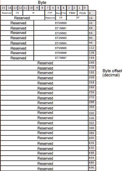
The currently executing task may or may not include the execution of FP or MMX instructions. When the timeslice for the current task expires, the timer interrupt causes a task switch back to the OS scheduler. Before actually resuming execution of the scheduler, however, the processor automatically saves the register set associated with the task being suspended into that task's TSS. The FP/MMX register set (they are one and the same) are not automatically saved, however. Rather, the scheduler uses the FSAVE instruction to save the FPU's register set in a data structure (see Figure 28-2 on page 713) associated with the task just suspended. Conversely, when the suspended task is restarted later in time, the FRSTOR instruction is used to reload the FPU's register set with its original contents.
Figure 28-2. FSAVE/FRSTOR Data Structure
Preparing for the Pentium® III's Introduction of SSE
When a new feature is introduced in a processor, it typically takes OS vendors a while to incorporate support for it. Two new instructions introduced in the Pentium® II processor were not required by the architecture at that time. They are backward-compatible with the FSAVE and FRSTOR instructions. In addition to saving and restoring the contents of the FPU's registers, they also save and restore the new SSE register set to be implemented on the Pentium® III processor in support of the SSE instruction set. These two new instructions are:
FXRSTOR. Restore the FPU and SSE registers from a memory data structure to the FPU and SSE register sets.
FXSAVE— Store the FPU and SSE register sets to a memory data structure.
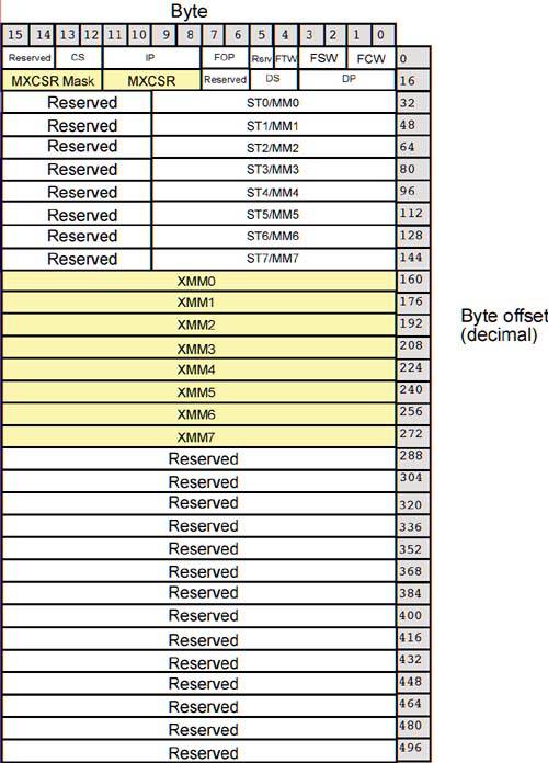
The data structure template is shown in Figure 28-3 on page 717. The SSE-related save fields are:
The contents of the MXCSR (the SSE Control Status Register) are saved in bytes 8 through 11 of the second row.
MXCSR_MASK (32 bits). See “The MXCSR Mask Field” on page 716 for a description of this field.
The contents of the eight, 128-bit XMM registers are saved in rows 11 through 17.
Figure 28-3. FXSAVE/FXRSTOR Data Structure
A detailed description of these two instructions can be found in “The FXRSTOR Instruction” on page 715 and “The FXSAVE Instruction” on page 715.
A detailed description of SSE can be found in “SSE Introduced” on page 748 and in “The Streaming SIMD Extensions (SSE)” on page 758.
When Executed on the Pentium® II Processor
When either of these instructions are executed on the Pentium® II processor, they are 100% compatible with the FSAVE and FRSTOR instructions—i.e., they only save and restore the FPU's register set.
Detecting the FP/SSE Save/Restore Capability
The programmer can determine if a processor supports this instruction pair by executing a CPUID request type 1 and verifying that the EDX[FXSR] bit is set to one (see Figure 28-1 on page 708).
The FXSAVE Instruction
When executed, the FXSAVE instruction writes the current FPU and SSE registers sets to a 512 byte memory data structure aligned on a 16-byte address boundary (see Figure 28-3 on page 717). Unlike FSAVE/FNSAVE, the processor retains the content of the FP SSE register sets after the registers have been saved. This instruction has been optimized to maximize FPU/SSE save performance.
The FXSAVE instruction is used when an OS needs to perform a context switch or when an exception handler needs to use the FPU and SSE register sets.
With the exception of the FPU's 16-bit Tag Word (FTW) field, bytes 0-159d of the memory data structure are identical to the format used by the FSAVE instruction. Unlike FSAVE, FXSAVE only saves an 8-bit version of the FTW register (where eight, 2-bit fields indicate whether or not the eight FP data registers contain valid data). Bit 0 = 1 if FP data register ST0 contains valid data and 0 if it doesn't, bit 1 = 1 if FP data register ST1 contains valid data and 0 if it doesn't, etc.
Note that on page-Table 3-133303 in the IA32 Intel® Architecture Software Developer's Manual Volume 2 Instruction Set Reference erroneously shows the FTW register saved in byte 5 of the first row and shows byte 4 blank. The FTW register is saved in byte 4 and byte 5 should be shown as reserved.
The FXRSTOR Instruction
When executed, the FXRSTOR instruction reloads the FPU and SSE register sets from the specified 512 byte data structure (aligned on a 16-byte address boundary) in memory (see Figure 28-3 on page 717). This data structure was saved by a previous execution of the FXSAVE instruction (see the previous section).
Three fields in the FPU save area contain reserved bits that are not indicated in Figure 28-3 on page 717:
In the FOP (FP Opcode) field, the lower 11-bits contain the opcode while the upper five bits are reserved. Note that the Fopcode register was not implemented until the advent of the Pentium® 4 processor.
The IP (Instruction Pointer) and DP (Data Pointer) fields:
- In 32-bit mode, no bits are reserved and it contains the 32-bit EIP-offset.
- In 16-bit mode, the lower 16-bits contain the IP-offset and the upper 16-bits are reserved.
Unlike FRSTOR, FXRSTOR does not cause an exception when loading an image from memory that contains a pending exception bit set to one in the FP Status Word (FSW) register. The next occurrence of this unmasked exception will result in the error exception being generated. It also does not flush any pending FPU exceptions. To check and raise exceptions when reloading the FPU and SSE register sets from a data structure, the programmer must execute the FWAIT instruction after the FXRSTOR instruction.
The MXCSR Mask Field
There are some reserved bits in the SSE Control Status register (i.e., MXCSR) that may be used in future IA32 processors. An attempt to set any reserved bits to one results in the generation of a GP exception.
When the FXSAVE instruction is executed, the processor deposits a value into the MXCSR_MASK field that indicates which bits of the MXCSR register are reserved. There are two possibilities:
If the default value 00000000h is stored in this field, it indicates that the processor does not support the DAZ bit (Denormals Are Zero is bit 6 in MXCSR; this bit was not implemented until the advent of the Pentium® 4 processor) and the programmer should assume a mask value of 0000FFBFh (bit 6 is cleared). The Pentium® III processor would return the default value of 00000000h because it did not implement the MXCSR[DAZ] bit. The Pentium® 4 processor, on the other hand, does implement the MXCSR[DAZ] bit, so it would not return the default value of 00000000h. Rather, it would return the value 0000FFFFh indicating that none of the MXCSR bits are reserved.
If a non-zero value is stored in this field, then the programmer should use the stored value as the mask value.
The recommended procedure for obtaining the mask value is as follows:
1. | Establish a 512-byte FXSAVE area in memory and zero it. |
2. | Execute the FXSAVE instruction supplying the start address of the data structure as the input parameter. |
3. | The processor has deposited the value in the MXCSR_MASK field in the FXSAVE image (bytes 28 through 31). |
If the mask (the default value of 0000FFBFh or the non-zero value deposited in the MXCSR_MASK field) is AND'd with a value to be written into the MXCSR register, the resulting value will have all reserved bits cleared to zero, guaranteeing that a GP exception will not be generated when the value is written to the MXCSR register.
The mask bits that are set to one indicate MXCSR features (i.e., bits) that are supported, so they can be thought of as feature flags for identifying the processor's SSE capabilities.