
Caching from SM Memory
Background
It is important to note that to the processor's caches, a memory address is a memory address: the caches do not differentiate between accesses to SM RAM and to regular system memory. This being the case, if the memory address range that is used to access SM RAM (while the processor is in SMM) partially or fully overlaps an address range in system memory that holds OS and/or application information, then one of the following two strategies must be employed:
The overlapping memory address range can be designated as UC memory in the MTTRs. The processor will not cache any information from SM RAM or from regular system memory.
The overlapping memory address range can be designated as cacheable memory (i.e., WP, WT or WB) in the MTRRs. The processor is then enabled to cache information from regular system memory when it is operating in Real Mode or Protected Mode, and from SM RAM when it is operating in SMM. This can result in better performance while operating any of the three modes. There is a catch, however.
Consider the following scenario:
Assume that SM RAM overlaps with regular system memory in the A0000000h through A000FFFFh memory address range (any range could be used in the example).
The overlapped address range has been marked cacheable (i.e., WP, WT or WB) in the MTRRs.
The processor has been operating in Protected Mode and has cached some information (code and/or data) from the overlapped address range.
An SMI occurs, switching the processor into SMM.
While in SMM, the processor performs a read access from the overlapped address range for the first time since entering SMM. This should result in a cache miss, but instead, it hits on a line that was cached from that location in regular system memory. The requested information is sourced from the cache.
This is WRONG! The processor should have performed the memory access on the FSB to fetch the line from SM RAM. The SM handler incorrectly receives data or code that was originally fetched from regular system memory and, as a result, the SM handler does not function correctly.
In this scenario, the cache must be flushed on entry to and exit from SMM. While this results in a big performance dip due to the cache flush and the subsequent cache misses that result, everything will work correctly.
The Physical Mapping of SM RAM Accesses
How the address ranges in SM RAM address space are actually mapped to physical memory chips is system design-specific. Here are several examples:
Refer to Figure 60-4 on page 1489. The chipset can direct the entire range of SM RAM addresses to an area of system RAM memory that will never be used by the OS and/or applications programs. In this case, the entire range can be designated as cacheable memory (WP, WT or WB; note that the Intel® documentation refers to WC as cacheable, but it is not) in the MTRRs (so as to achieve the best possible performance by caching SM RAM information).
Refer to Figure 60-5 on page 1490. The chipset can direct the entire range of SM RAM addresses to RAM storage that is implemented using totally separate and distinct RAM chips from the system RAM memory used by the OS and/or applications programs. The address range may be an address range that is also used (by normal memory accesses) to access system RAM memory. The entire range is designated as uncacheable memory (UC) in the MTRRs.
Refer to Figure 60-6 on page 1491. The chipset can direct any access within the SM RAM address space to an area of system RAM memory that is also used by the OS (but not at the same time, of course). This area would be designated as UC memory in the MTRRs.
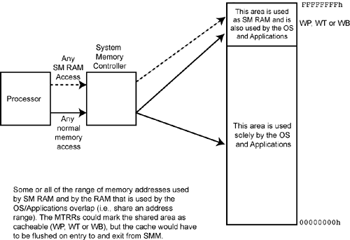
Refer to Figure 60-7 on page 1492. The chipset can direct any access within the SM RAM address space to the system RAM memory that is also used by the OS and/or applications programs and the MTRRs could designate the entire address range as cacheable (so as to achieve the best possible performance by caching OS/application information as well as SM RAM information). However, the cache would have to be flushed upon entry to and exit from SMM (by executing the WBINVD instruction).
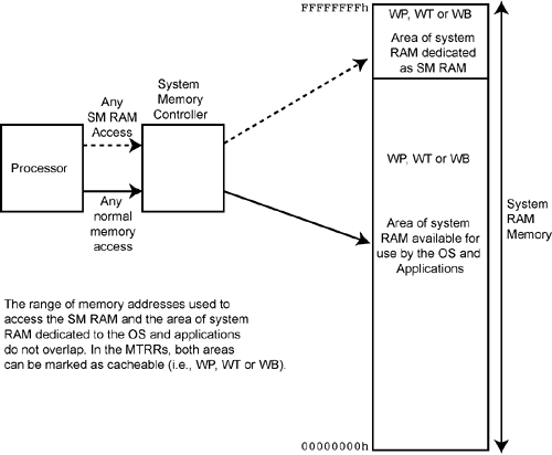
Refer to Figure 60-8 on page 1493. This is the scenario recommended by Intel® for all IA32 processors starting with the Pentium® Pro. While part of the SM RAM address range overlaps with regular memory used by the OS and applications, another part of the SM RAM memory space is dedicated to SM RAM and is never used by the OS or applications. The overlapped portion of the address space overlaps with video memory (which is usually in low memory) and is marked as UC memory in the MTRRs. The initial entry point to the SM handler is located in this shared area. Very soon after entering SMM, however, the SM handler code performs a jump to the main portion of the handler which is located in the memory range that is dedicated to SM RAM and is never used by the OS and applications. This dedicated area can be designated as cacheable memory (i.e., WP, WT or WB) to achieve good performance while in SMM.


FLUSH# and SMI#
Description
This discussion relates to the situation described in “Background” on page 1487. Prior to the advent of the Pentium® 4 processor, all IA32 processors starting with the Pentium® implemented the following two inputs:
FLUSH#. When asserted by the chipset, it caused the processor to write back all of its modified lines to memory and then delete all of the lines in its caches. After completion of the cache flush, the processor would generate a Special transaction on its FSB and output the Flush Acknowledge message on its Byte Enables. This would inform the chipset that the flush had been completed.
SMI#. When asserted by the chipset, it caused the processor to switch from Real Mode or Protected Mode into SMM.
Both of these inputs were treated as interrupts to the processor with FLUSH# having a higher priority than SMI#. A system could be designed so that it would assert SMI# and FLUSH# to the processor simultaneously. The processor would service the FLUSH# first, purging its caches of the information cached from regular system memory, and would then service the SMI# and enter SMM. The following timing constraints had to be met:
In a system where FLUSH# and SMI# were synchronous and the set up and hold times were met, FLUSH# and SMI# could be asserted in the same clock.
In asynchronous systems, FLUSH# had to be asserted at least one clock before SMI# to guarantee that FLUSH# was serviced first.
Before executing the RSM instruction to exit SMM, the SM handler would have to execute the WBINVD instruction to flush the information that had been cached from SM RAM.
A Cautionary Note Regarding the Pentium®
In systems based on the Pentium® processor that used FLUSH# to purge the caches before entering SMM, the processor would prefetch at least one cache line (and possibly more than one) from regular system memory after it generated the Special transaction to output the Flush Acknowledge cycle, but before it started accessing SM RAM. The system design had to ensure that these lines were not cached by deasserting the processor's KEN# input during those cache line fetches.