
The Cartridge
The Pentium® and Pentium® Pro Sockets
The Pentium® and Pentium® Pro processors utilized PGA (i.e., Pin Grid Array) packages and were installed into a PGA socket on the system board. The Pentium® sockets were referred to as sockets 1 through 7, with socket 7 being the de facto standard on most Pentium® system boards. The Pentium® Pro processor implemented the socket 8 PGA. System board designers could license Socket 8 from Intel®, but processor designers could not.
The Problem
It stands to reason that Intel® must have had a good reason for switching from the compact PGA package to the rather large cartridge. At that time, the silicon wafer and die layout processes in use were rather coarse when compared to today's technologies. This made it impossible to include a large number of transistors on the processor die. That was Intel®'s original impetus for using the dual-PGA package (see Figure 26-1 on page 662) used on the Pentium® Pro. The dual-PGA package, however, was not an elegant, long-term solution. In order to increase the L2 cache size, Intel® went to the cartridge format.
Figure 26-1. The Pentium® Pro's Dual-PGA Package

Once the silicon wafer and layout technologies progressed to a sufficiently small size permitting the L2 cache to be integrated onto the processor die, it was no surprise that Intel® switched from the cartridge back to socketed processors. The cartridge format was expensive to produce, large, and consumed a substantial amount of system board real estate.
The Pentium® II Cartridge
With the advent of the Pentium® II processor, Intel® switched to a Single-Edge Cartridge (i.e., SEC) processor package. The system board incorporated a single, in-line connector into which the processor card was installed. This was referred to as the Slot 1 connector. System board designers could license Slot 1 from Intel®, but processor designers could not.
The processor core and L2 Cache were contained on a card, referred to as the substrate, that installed into the Slot 1 connector. The substrate was completely enshrouded within a cover that provided EMI shielding and a metal thermal plate used to dissipate processor heat through a heat sink attached to the thermal plate. Figure 26-3 on page 664 illustrates a front view of the SEC cartridge with the cover in place, Figure 26-2 on page 663 illustrates a side view, and Figure 26-4 on page 665 shows three views. Note that the cover is located over the rear (non-processor) side of the substrate, while the thermal plate is attached to the processor side of the substrate. When Intel® originally presented the cartridge to its customer base for comments, neither the processor core nor any of its support logic was visible. From a marketing perspective, the end-customer had grown accustomed to seeing the processor chip. To address this perception, Intel® included a label with a picture of the processor core die on the cover (see Figure 26-3 on page 664).
Figure 26-3. The SEC Cartridge Cover

Figure 26-2. SEC Cartridge Side-View
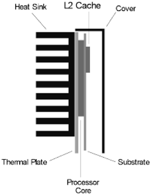
Figure 26-4. The Cover and Views of Both Sides of the Substrate

The SEC Substrate: the Processor Side
General
Figure 26-5 on page 667 illustrates the front side of the substrate. It contains the processor core as well as two of the four SRAMs that comprise the L2 Cache's four data banks used for storing lines of memory information. It also contains a number of passive components not pictured in the illustration.
Figure 26-5. Processor Core Side of SEC Substrate

Processor Core
The processor core was implemented in a plastic LGA (Land Grid Array) package with a metal heat spreader attached to it. The LGA package was similar to a Ball Grid Array, or BGA package utilizing small pads but no solder balls.
The LGA package was mounted on a small circuit board (see Figure 26-5 on page 667) attached to the substrate. When the cartridge was assembled, thermal grease was applied to the processor core's heat spreader and the thermal plate was placed in contact with the heat spreader (see Figure 26-2 on page 663). The heat sink, in turn, was attached to the thermal plate.
The SEC Substrate: the Non-Processor Side
The other side of the substrate (pictured in Figure 26-6 on page 668) contained the L2 Cache's tag SRAM (i.e., the L2 Cache directory) and the other two data SRAMs. It also contained a numbered of passive components not pictured in the figure.
Figure 26-6. Non-Processor Side of SEC Substrate

Cartridge Block Diagram
Figure 26-7 on page 670 illustrates the basic relationship of the device's located on the substrate. As with the Pentium® Pro processor, the processor core was linked to the outside world via two buses:
The Backside Bus (BSB) provided a dedicated path between the core and the L2 Cache.
The cartridge was installed into the Slot 1 system board connector, giving it access to the external, or front side, bus (FSB).
Figure 26-7. Simplified Block Diagram of the Pentium® II Processor Cartridge
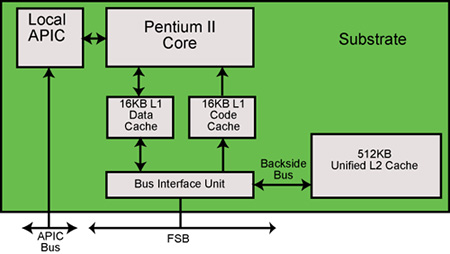
Like the Pentium® Pro, the Pentium® II processor core could simultaneously transfer data on both the BSB and the FSB. However, the physical length of the traces between the Pentium® Pro processor core and its L2 Cache was extremely short, permitting the BSB to operate at the full processor core speed. The Pentium® II processor's BSB, on the other hand, was physically much longer, necessitating a slower BSB speed. As a result, the BSB operated at one-half the processor core speed. As an example, the 266MHz Pentium® II had a BSB speed of 133MHz. Because the slower BSB speed adversely affected processor core performance when accessing the L2 Cache, the L1 cache sizes were double those found in the Pentium® Pro processor. The increased L1 cache size permitted the processor core to keep more memory-based information close to its heart, decreasing the number of accesses that needed to be made to the L2 Cache. For additional information, see “Dual-Independent Bus Architecture (DIBA)” on page 658, and “The Processor Core and Bus Frequencies” on page 676.
The L2 Cache
The L2 Cache had the following characteristics:
It was a unified code/data cache.
It was implemented using discrete SRAM chips mounted on the cartridge substrate.
It was a 4-way, set-associative cache.
It was 512KB in size on the Pentium® II processor.
It was available in sizes of 512KB, 1MB or 2MB on the Pentium® II Xeon processor.
It implemented the full MESI coherency protocol.
The cache line size was 32 bytes.
It was a non-blocking cache.