
Pentium® 4 Processor Basic Organization
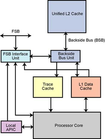
Refer to Figure 35-1 on page 840. The Pentium® 4 processor includes the following major subsystems:
The processor core. This is the heart of the beast: the instruction fetch, decode, execute engine. It is responsible for the following:
- Instruction fetch.
- Branch prediction.
- Parsing of the IA instruction stream.
- Decoding of IA instructions into primitive, fixed-length instructions (referred to as micro-ops, or μops).
- Mapping accesses for the small IA data register set to a larger physical register set.
- Dispatch, execution and retirement of μops.
The Local APIC. This unit receives interrupt requests from sources local to the processor as well as from remote sources (e.g., other processors and the IO APIC) and is also capable of sending interrupt messages to other processors, or to the IO APIC(s) within the chipset. Unlike the Pentium® and P6 processor families (which implemented the 3-wire APIC bus), the Local APIC communicates with the Local APICs in other processors and with the IO APIC(s) in the chipset via interrupt message transactions performed on the FSB.
The L1 Data Cache. This unit caches data from system memory to expedite the execution of load and store operations. In the event of a cache miss, the request is forwarded upstream to the L2 Cache over the BSB for fulfillment.
The Trace Cache. Unlike the earlier IA32 processors, the L1 Code Cache in the Pentium® 4 does not cache legacy IA32 instructions. Rather, it caches the instructions after they have been decoded into μops. In the event of a cache miss, the request is forwarded upstream to the L2 Cache over the BSB for fulfillment.
The Back Side Bus (BSB) interface connects the L2 Cache to the L1 caches as well as to the FSB interface unit (and to the on-die L3 Cache if the processor implements one).
The on-die L2 Cache. The L2 Cache is on the processor die in all models of the Pentium® 4 processor family. This unit services loads and stores that miss the processor's L1 caches. In the event of a cache miss, the request is forwarded upstream to the FSB (or to the on-die L3 Cache if the processor implements one).
Optionally, an on-die L3 Cache. As of this writing, an on-die L3 cache is implemented on the Pentium® 4 Extreme, all Xeon MP processors, and later model Xeon DP processors.
The Front Side Bus (FSB) interface. The FSB connects the processor to the outside world. The processor uses it to communicate with other devices, to snoop memory transactions initiated by other entities, and to send and receive interrupt messages.
Figure 35-1. Simplified Pentium® 4 Block Diagram
In the event of a miss on either of the L1 caches, the L2 Cache can be accessed via the BSB at the same time that the processor (or an another FSB agent) is using the FSB. This is referred to as the Dual Independent Bus Architecture, or DIBA.