
The Streaming SIMD Extensions (SSE)
Why?
The single most important impetus behind the Streaming SIMD Extensions (SSE) was to achieve a significant performance boost when executing multimedia applications. To this end, Intel® needed to:
Extend the SIMD model to include SIMD FP capability (as MMX made SIMD integer operations possible).
Provide new instructions specifically tailored to boost the performance of multimedia applications.
Enhance memory write operations and to make more efficient use of the FSB.
It should be noted that applications other than multimedia applications can also realize significant benefit from the new SSE feature set.
Detecting SSE Support
Refer to Figure 31-1 on page 759. The programmer can determine if a processor supports the SSE instruction and register set by performing a CPUID request type 1 and checking that EDX[SSE] = 1.

The SSE Elements
The implementation of SSE was accomplished by adding the following elements to the processor architecture:
70 new instructions (SSE instruction set) were added to the instruction set.
Eight, 128-bit data registers were added to the architecture (see Figure 31-2 on page 760). Unlike the MMX registers which are aliased over the lower 64 bits of each of the x87 FPU's data registers, the SSE data registers are implemented as separate registers.
A Control/Status register (MXCSR; Figure 31-2 on page 760) to control the SSE FP SIMD capability and to indicate its status via the error status bits.
A new SIMD FP exception was added to report SSE SIMD FP errors to the OS.

The SSE instructions can be divided into the following categories:
SIMD FP instructions that simultaneously operate on four, 32-bit, Single Precision (SP) FP numbers.
Scalar FP instructions. First, a definition of scalar: a single number, as opposed to a vector or matrix of numbers. As an example, scalar multiplication refers to the operation of multiplying one number (one scalar) by another and the term scalar is used to differentiate this from matrix math operations.
Cacheability instructions including prefetches into different levels of the cache hierarchy.
Control instructions.
Data conversion instructions.
New media extension instructions such as the PSAD and the PAVG that accelerate encoding and decoding, respectively.
The SSE Data Types
General
Each 128-bit XMM register can hold:
16 bytes packed into an XMM register or into a memory variable, or
8 words packed into an XMM register or into a memory variable, or
4 dwords packed into an XMM register or into a memory variable, or
2 qwords packed into an XMM register or into a memory variable, or
Four 32-bit Single Precision (SP) FP numbers (see Figure 31-3 on page 765) packed into an XMM register or into a memory variable.

The 32-bit SP FP Numeric Format
Background
The new data type introduced with the advent of SSE is the 32-bit SP FP numeric format and it fully complies with the definition found in the IEEE Standard 754 for Binary FP Arithmetic. It should be noted that although this data type is new to the IA32 SIMD model, it is not new. It was defined in the 1980s and has been supported by the Intel® x87 FPU for many years. The x87 FPU, however, stores all FP numeric values in memory in the 80-bit (10 byte) DEP (Double Extended Precision) format (see “The FP Data Operand Format” on page 443). On reading a value from memory, the x87 can perform computations on the value in its native DEP form or, prior to performing a computation, can internally convert it into the 32-bit SP or the 64-bit DP form (see “DP FP Number Representation” on page 1334). When a numeric value is stored back to memory, however, the x87 FPU automatically converts it to the DEP form before storing it. The following is a brief tutorial on the 32-bit SP FP format.
A Quick IEEE FP Primer
The author would like to stress that this is not meant to be a comprehensive tutorial on the IEEE FP specification. Rather, it is meant to familiarize a reader who is not conversant in the FP vernacular with the major concepts and terms necessary to understand the basics.
A FP value represented in the IEEE FP format is computed as follows:
x.yyyyy * 2zth
where the digit to the left of the decimal point (x) is implied and is assumed to be one for all numbers (positive or negative) except for:
- Zero and
- Numbers (irrespective of their sign, either positive or negative) that are less than 1 but greater than 0 (e.g., +0.1242, +0.98, -0.548, -0.13, etc.). These are referred to as denormal numbers (and are also referred to as tiny numbers).
- In both of these cases, the implied digit is assumed to be 0.
The range of all possible real numbers that can be represented using this format are limited by the width of the y field (referred to as the mantissa or significand field) and the z field (the exponent field). As shown in Figure 31-3 on page 765, the 32-bit format uses an 8-bit exponent field and a 23-bit mantissa field.
The IEEE specification defines the range of possible real numbers as falling into the following categories (ranging from most positive to most negative):
- + ∞
- +1.n, where n is > 0 (referred to as positive normal numbers)
- +0.n, where n is > 0 (referred to as positive denormal numbers)
- +0
- -0
- -0.n, where n is > 0 (referred to as negative denormal numbers)
- -1.n, where n is > 0 (referred to as negative normal numbers)
- - ∞
The specification also expresses the concept of values that are not real numbers (referred to as NaNs for Not a Number). They are categorized as follows:
- -
SNaN (Signaling NaN).
A SNaN is a NaN with the most significant fraction bit cleared to zero. SNaNs generally signal an FP Invalid Operation exception whenever they appear as operands in arithmetic operations. SNaNs are typically used to cause a FP exception. The processor never generates an SNaN as a result of a FP operation. Rather, software would insert a SNaN to cause a FP exception.
- -
QNaN (Quiet NaN).
A QNaN is a NaN with the most significant fraction bit set to one. The processor's FP execution units allow QNaNs to propagate through most arithmetic operations without causing a FP exception.
The 32-bit SP FP Format
As illustrated in Figure 31-3 on page 765, a 32-bit, FP number is represented as follows:
- Bit 31 is the sign bit and indicates whether the value represented is a positive (0) or a negative (1) value.
- Bits [30:23] is the exponent field.
- Bits [22:0] is the mantissa field and represents the fractional part of the number that is to be multiplied by 2exponent.
- The digit to the left of the decimal point is implied and is either a 0 or a 1 (as mentioned earlier).
Representing Special Values
Table 31-1 on page 763 defines how special values are represented.
An Example
The following example presents the steps necessary to convert the base 10 number +100.25 into a 32-bit SP FP number.
1. | Converting the whole number (10010) to binary yields11001002. | ||||||||||||||||||||||||||||||||||||||||||||||||||||||||||||||||||||||||||||||||||||||||||||||||||||||||||||||||||||||||||||||||||||||||||||||||||||||||||||||||
2. | Converting the fractional part (.2510) to binary yields .012. The first bit position to the right of the decimal place represents the value .510 (1 divided by 2), the 2nd bit the value .2510 (1 divided by 4), the third the value .12510 (1 divided by .0625), etc. | ||||||||||||||||||||||||||||||||||||||||||||||||||||||||||||||||||||||||||||||||||||||||||||||||||||||||||||||||||||||||||||||||||||||||||||||||||||||||||||||||
3. | Convert the full binary representation of the number to the normalized form (i.e., as in scientific notation): +1100100.012 = +1.100100012 * 26(base 10) | ||||||||||||||||||||||||||||||||||||||||||||||||||||||||||||||||||||||||||||||||||||||||||||||||||||||||||||||||||||||||||||||||||||||||||||||||||||||||||||||||
4. | Convert the exponent. When using the 32-bit SP FP format, the exponent is generated by adding a bias value of 12710 to the base 10 exponent generated in the previous step (610). In this case, 12710 + 610 = 13310. That number is then converted to binary: 13310 = 100001012. | ||||||||||||||||||||||||||||||||||||||||||||||||||||||||||||||||||||||||||||||||||||||||||||||||||||||||||||||||||||||||||||||||||||||||||||||||||||||||||||||||
5. | Finally, assemble the components using the 32-bit SP FP template (see Table 31-2 on page 764). If necessary, pad the exponent with zeros on the left so as to make it a full 8 bits in width. In addition, if it is necessary, pad the mantissa with zeros on the right to make it a full 23 bits in width.
| ||||||||||||||||||||||||||||||||||||||||||||||||||||||||||||||||||||||||||||||||||||||||||||||||||||||||||||||||||||||||||||||||||||||||||||||||||||||||||||||||
Another Example
The following example presents the steps necessary to convert the base 10 number +178.125 into a 32-bit SP FP number.
1. | Converting the whole number (17810) to binary yields 101100102. | ||||||||||||||||||||||||||||||||||||||||||||||||||||||||||||||||||||||||||||||||||||||||||||||||||||||||||||||||||||||||||||||||||||||||||||||||||||||||||||||||
2. | Converting the fractional part (.12510) to binary yields .0012. The first bit position to the right of the decimal place represents the value .510 (1 divided by 2), the 2nd bit the value .2510 (1 divided by 4), the third the value .12510 (1 divided by .0625), etc. | ||||||||||||||||||||||||||||||||||||||||||||||||||||||||||||||||||||||||||||||||||||||||||||||||||||||||||||||||||||||||||||||||||||||||||||||||||||||||||||||||
3. | Convert the full binary representation of the number to the normalized form (i.e., as in scientific notation): +10110010.0012 = +1.01100100012 * 27(base 10) | ||||||||||||||||||||||||||||||||||||||||||||||||||||||||||||||||||||||||||||||||||||||||||||||||||||||||||||||||||||||||||||||||||||||||||||||||||||||||||||||||
4. | Convert the exponent. When using the 32-bit SP FP format, the exponent is generated by adding a bias value of 12710 to the base 10 exponent generated in the previous step (710). In this case, 12710 + 710 = 13410. That number is then converted to binary: 13410 = 100001102. | ||||||||||||||||||||||||||||||||||||||||||||||||||||||||||||||||||||||||||||||||||||||||||||||||||||||||||||||||||||||||||||||||||||||||||||||||||||||||||||||||
5. | Finally, assemble the components using the 32-bit SP FP template (see Table 31-3 on page 765). If necessary, pad the exponent with zeros on the left so as to make it a full 8 bits in width. In addition, if it is necessary, pad the mantissa with zeros on the right to make it a full 23 bits in width.
| ||||||||||||||||||||||||||||||||||||||||||||||||||||||||||||||||||||||||||||||||||||||||||||||||||||||||||||||||||||||||||||||||||||||||||||||||||||||||||||||||
Accuracy vs. Fast Real-Time 3D Processing
SSE includes two FP arithmetic modes:
One emphasizes IEEE compliance and exact, single precision results.
The other emphasizes computational speed at the expense of a slight loss in precision. The mode selection is controlled by the MXCSR[FTZ] bit (FTZ = Flush to Zero). Setting this bit to one selects FTZ mode, while clearing it selects the IEEE-compliance mode of operation.
FTZ mode is well-suited for real-time applications. During computation, it returns a zero result in an underflow situation if the reporting of SSE SIMD FP exceptions is masked. Most real-time 3D applications place the emphasis on speed and are not sensitive to a slight loss in precision.
The SSE Register Set
The registers associated with SSE are:
Eight, 128-bit data registers (XMM[7:0]). Unlike the MMX registers which are aliased over the lower 64 bits of each of the x87 FPU's data registers, the SSE data registers are implemented as separate registers.
A Control/Status register (MXCSR) to control the SSE FP SIMD capability and to indicate its status via a series of error status bits.
The sections that follow provide a description of the SSE-related registers.
The XMM Data Registers
As stated earlier, each of the 128-bit XMM registers can hold:
16 bytes packed into the XMM register, or
8 words packed into the XMM register, or
4 dwords packed into the XMM register, or
2 qwords packed into the XMM register, or
Four 32-bit SP FP numbers (see Figure 31-3 on page 765) packed into the XMM register.
The MXCSR
The MXCSR (the SSE Control/Status register) is pictured in Figure 31-4 on page 769 and its bit fields are described in Table 31-4 on page 767.

| Field Name | Width (in bits) | Description |
|---|---|---|
| FP Exception Error Status Bits | 6 bits | When performing a SIMD FP operation, the processor may experience any of six different types of error conditions. These six error status bits are each associated with one of those error conditions. They are “sticky” bits; after a bit is set, it remains set until explicitly cleared using the LDMXCSR or FXRSTOR instruction to write zeroes into them. All six of these error types (except the Denormal Operand error) are defined in IEEE Standard 754, and they are the same exceptions that are generated with by the x87 FPU. All of the SIMD FP exceptions are precise (i.e., they are generated as soon as the instruction is executed). Each of the six exception conditions has a corresponding mask bit (IM, DM, ZM, OM, UM, and PM) in MXCSR. The mask bits can be set using either the LDMXCSR or FXRSTOR instruction and the mask and error bits can be read using either the STMXCSR or FXSAVE instruction. If an unmasked SIMD FP exception is generated and CR4[OSXMMEXCEPT] = 1 (see “Enable the SSE SIMD FP Exception” on page 771), the processor generates the SIMD FP exception. If CR4[OSXMMEXCEPT] = 0, the processor generates an Invalid Opcode exception on the first SSE instruction that detects a SIMD FP exception condition. |
| FP Exception Mask Bits | 6 bits | Bits 7 through 12 provide individual mask bits for the SIMD FP exceptions.
|
| FP Rounding Control | 2 bits |
|
| FTZ | 1 | Enables Flush to Zero mode (refer to “Accuracy vs. Fast Real-Time 3D Processing” on page 765). Controls the masked response to a SIMD FP underflow condition. When the underflow exception is masked and FTZ Mode is enabled, the processor performs the following operation when it detects a FP underflow condition:
|
| DAZ | 1 | The Denormals As Zeros bit was not implemented until the Pentium® 4. See “Your Choice: Accuracy or Speed” on page 1336 for more information. |
Loading and Storing the MXCSR
The LDMXCSR and STMXCSR instructions are used to load the MXCSR from memory, or to store its contents to memory.
Saving and Restoring the Register Set
The FXSAVE instruction is used to save the contents of the FP/MMX and the SSE register sets into a data structure in memory.
The FXRSTOR instruction is used to restore the FP/MMX and the SSE register sets from a data structure in memory. These two instructions were actually added in the Pentium® II processor and a detailed description can be found in “FP/SSE Save/Restore Instruction Pair” on page 712.
OS Support for FXSAVE/FXRSTOR, SSE and the SIMD FP Exception
General
An OS may or may not implement the following:
The OS may or may not enable the FXSAVE and FXRSTOR instructions to save the SSE register set in addition to the FPU registers set.
The OS may or may not support the use of the SSE instruction set.
The OS may or may not implement an SSE SIMD FP exception handler (i.e., the exception 19 handler).
The OS indicates (to application programs) whether or not it supports these features by appropriately setting or clearing two new bits in CR4 (see Figure 31-5 on page 771). The following two subsections describe the effects of these two bits.

Enable SSE/SSE2 and SSE Register Set Save and Restore
Refer to Figure 31-5 on page 771. The OS will set CR4[OSFXSR] bit to one if it supports:
the use of the FXSAVE and FXRSTOR instructions to save and restore both the FPU and SSE register sets, and
it also supports the use of the SSE instruction set (and, if this is any IA32 processor starting with the Pentium® 4, supports the use of the SSE2 instruction set).
Setting CR4[OSFXSR] to one enables the processor to execute the SSE (and, if this is any IA32 processor starting with the Pentium® 4, the SSE2) instruction set. The following SSE instructions are always enabled: PREFETCHh or SFENCE. On any IA32 processor starting with the Pentium® 4, the following SSE2 instructions are always enabled: PAUSE, LFENCE, MFENCE, MOVNTI, and CLFLUSH.
Setting CR4[OSFXSR] to one enables the FXSAVE and FXRSTOR instructions to save and restore the contents of the SSE register set along with the contents of the FPU/MMX register set.
Clearing CR4[OSFXSR] to zero has the following effects:
When the FXSAVE and FXRSTOR instructions are executed, they save and restore the contents of the FPU/MMX register set, but they may or may not (processor design-specific) save and restore the contents of the SSE register set.
The processor generates the Invalid Opcode exception whenever it attempts to execute any of the SSE instructions with the exception of the PREFETCHh or SFENCE instructions. These two instructions are always enabled.
On any IA32 processor (starting with the Pentium® 4) the processor generates the Invalid Opcode exception whenever it attempts to execute any of the SSE2 instructions with the exception of the PAUSE, LFENCE, MFENCE, MOVNTI, and CLFLUSH instructions. These five instructions are always enabled.
Enable the SSE SIMD FP Exception
Refer to Figure 31-5 on page 771. The OS will set CR4[OSXMMEXCPT] to one if it implements the SSE FP SIMD exception handler (the exception 19 handler).
SSE SIMD FP exceptions are only generated by SSE (and, starting with the Pentium® 4, SSE2) SIMD FP instructions. If CR4[OSXMMEXCPT] is cleared to zero, the processor generates an Invalid Opcode exception whenever it detects an unmasked SIMD FP exception.
SIMD (Packed) Operations
Much like the integer operations performed by MMX (see “MMX SIMD Solution” on page 524), four SP FP operations can be executed simultaneously using the SSE SIMD FP capability. Figure 31-6 on page 772 illustrates a SIMD add operation on four, 32-bit SP FP numbers packed in XMM0 and another four packed in XMM1. In the example, the result of the four separate add operations is deposited in XMM0.
Figure 31-6. Example SSE SIMD FP Operation on Packed 32-bit SP FP Numbers

All instruction mnemonics for packed SP FP operations have the ps (packed SP FP) suffix appended after the operation type (e.g., ADDPS = add packed SP FP numbers).
Scalar Operations
Unlike a packed operation, a scalar operation only operates on the least-significant SP FP numeric value in an XMM register. As an example, Figure 31-7 on page 773 illustrates a SIMD scalar operation wherein the least-significant SP FP numeric value in each of the two XMM registers are added and the result is deposited in the least-significant part of the destination XMM register. The upper three, 32-bit SP FP numbers in each of the two registers are unaffected.
Figure 31-7. Example SSE SIMD Scalar Operation

Cache-Related Instructions
The SSE instruction set also includes an instruction that can be used to prefetch a line into a specified cache level before the data is actually needed. The PREFETCHh instruction is described in “Overlapping Data Prefetch with Program Execution” on page 773.
In addition, streaming store (i.e., memory write) instructions are also included (a description can be found in “Streaming Store Instructions” on page 776).
Overlapping Data Prefetch with Program Execution
When the processor executes a load (i.e., a memory data read) within an area of memory designated as cacheable, the processor core performs a lookup in the L1 Data Cache. If the line is not in the cache, the request is forwarded to the L2 Cache for a lookup. If the requested line is not present in the L2 Cache, the processor must forward the request to system memory over the FSB for fulfillment. The FSB runs at a fraction of program execution speed, so the line fetch from system memory takes a considerable amount of time. Meanwhile, the load is stalled for that entire length of time. If program execution results in a considerable number of load misses, the processor core begins to stall. Obviously, if the execution of a load results in a cache miss, the load completes very quickly and the program execution speeds benefits.
The Pentium® III processor added a new instruction, PREFETCHh, to increase the likelihood of a cache hit when the load is executed. Consider the following code fragment:
prefetchh
xxx
xxx
xxx
xxx
  .
  .
  .
load
The processor core treats the PREFETCHh instruction as a hint that the line specified by the instruction will probably be needed by the program in the future. Normally, when a load is executed, the processor core cannot retire it until the load completes (i.e., until the data has been fetched into the cache and the requested data that caused the miss has been placed in the target register). When the line fetch request caused by the execution of a PREFETCHh instruction is dispatched to the cache hierarchy for a lookup, however, it is considered completed and is retired immediately. Program execution continues. Meanwhile, the cache lookup(s) is performed and, in the event of a miss on all cache levels, the processor dispatches the line read request to system memory over the FSB for fulfillment. The line is returned from memory and is placed in the level of cache specified by the PREFETCHh instruction.
There are actually two benefits involved:
When the currently running program gets to the point where it must access any data item within the line that was prefetched, it may already be in the cache and the load or store can complete very quickly.
The program can specify into which cache level the line will be fetched. As an example, the programmer may specify that the prefetched line is to be placed only into the L2 Cache and not into the L1 Data Cache. As a result, the line is placed in the L2 Cache so the processor core has relatively quick access to it, but it is not placed in the L1 Data Cache. The L1 Data Cache therefore does not have to evict a line already in the cache in order to make room for the prefetched line. The PREFETCHh instruction helps prevent the unnecessary eviction of lines from the cache.
Currently, there are four forms of the PREFETCHh instruction as specified in Table 31-5 on page 776. The form is encoded into the machine level instruction using bits [5:3] of the instruction's ModR/M byte. A 3-bit field has eight possible values, so there is room for the future addition of up to four additional forms. The table makes reference to the terms temporal and non-temporal data:
Temporal data is data that the currently executing program will probably require access to in the near-term.
Non-temporal data is data that the currently executing program will probably not require access to in the near-term.
| Instruction Form | Description | Pentium® III Behavior | Pentium® 4 Behavior |
|---|---|---|---|
| PREFETCHT0 | Temporal data. Prefetch data into all levels of the cache hierarchy. | Model-specific whether it's placed in the L1 or L2 cache. | The line is placed in the L2 cache. |
| PREFETCHT1 | Temporal data with respect to L1 cache. Prefetch data into L2 and higher. | The line is placed in the L2 cache. | The line is placed in the L2 cache. |
| PREFETCHT2 | Temporal data with respect to L2. Prefetch data into L2 and higher. | The line is placed in the L2 cache. | The line is placed in the L2 cache. |
| PREFETCHNTA | Non-temporal data with respect to all cache levels. Prefetch data into non-temporal cache structure and into a location close to the processor, minimizing cache pollution. | The line is placed in the L1 cache. | The line is placed in the L2 cache. |
As noted in the table, it is processor design-specific into which cache level(s) the target line will be placed. In a case where the programmer must know into which cache level(s) the target line will be prefetched, the programmer must check the processor type (via the CPUID instruction) and must be aware of the processor-specific behavior when executing this instruction.
The following are additional characteristics of the PREFETCHh instruction:
The specification frequently refers to the PREFETCHh instruction. The h stands for the type of hint.
A specific processor implementation may ignore specific hint type(s).
If the linear-to-physical address translation selects a page that is not currently present in memory, the processor does not generate a Page Fault exception. Rather, it just treats the prefetch as a NOP.
If the data is already present in a cache level closer to the core than the level specified by the instruction, the instruction acts as a NOP.
The instruction does not affect the behavior of the program.
A prefetch from UC (Uncacheable) or WC (Write Combining) memory is ignored (because both are uncacheable).
The amount of data prefetched is design-dependent (i.e., it is the cache line size for the specified processor cache), but is always a minimum of 32 bytes.
Only placing data in the L1 preserves data currently resident in the L2 (and vice versa). If an L2 data line is cast out, obviously it is no longer available for fast access by the core. In addition, if the line being cast out is a modified line, it causes a writeback of the line on the FSB (consuming bus bandwidth).
It should be noted that the processor core can speculatively fetch and cache data from system memory regions that are assigned a memory type that permits speculative reads (i.e., WB, WT, WP and WC). Refer to “The Memory Types” on page 581 for a detailed description of the possible memory types. The PREFETCHh instruction is considered a hint to this speculative behavior. Because speculative fetching can occur at any time and is not tied to instruction execution, a PREFETCHh instruction is not ordered with respect to the fence instructions (MFENCE, SFENCE, and LFENCE) or to locked memory accesses. A PREFETCHh instruction is also unordered with respect to the CLFLUSH instruction, other PREFETCH instructions, or any other general instruction. It is ordered with respect to serializing instructions (see “Serializing Instructions” on page 1079) such as CPUID, WRMSR, OUT, and MOV CR.
Streaming Store Instructions
Introduction
When a store is performed to an area of memory that is designated as cacheable memory (i.e., it is WB, WT, or WP memory), the processor performs a lookup in its internal caches. The processor's handling of the memory write is defined by the type of memory as well as whether or not the cache lookup results in a hit or a miss. Table 31-6 on page 777 defines the processor's actions.
| Memory Type | Actions on a Cache Miss | Actions on a Cache Hit |
|---|---|---|
| WP | The write's start address and the bytes to be written are posted in the processor's Posted Memory Write buffer and are written to memory later. The line is not fetched from memory and placed in the cache. | The target byte(s) within the cache line are not updated. The write's start address and the bytes to be written are posted in the processor's Posted Memory Write buffer and are written to memory later. |
| WT | The write's start address and the bytes to be written are posted in the processor's Posted Memory Write buffer and are written to memory later. The line is not fetched from memory and placed in the cache. | The target byte(s) within the cache line are updated. In addition, the write's start address and the bytes to be written are posted in the processor's Posted Memory Write buffer and are written to memory later. |
| WB | The processor arbitrates for ownership of the FSB and performs a Memory Read and Invalidate transaction to fetch the line from system memory. This transaction type is sometimes referred to as a RWITM (Read With Intent To Modify) because the processor is fetching the line with the intent to store into it. It is also referred to as an RFO (Read For Ownership) for the same reason. When it receives the line, it places it in its cache, immediately stores into it and marks it Modified (M). If any other processor observing the RWITM transaction has a copy of the line:
| If the processor has a copy of the line, the line's current state dictates the processor's handling of the write:
|
Disadvantages:
| Disadvantages
|
The currently executing program may perform a store to an area of memory designated as WB memory, but the program may “know” that it will not be accessing any data within that line for quite a while. As can be seen in the table, this can have a number of negative consequences. One solution would be to designate the area of memory as some type other than WB. This, however, is a draconian solution in that, at some other point in time, the program may need the performance benefits yielded by designating the region as WB memory. Prior to the advent of the Pentium® III, this was the only solution.
A better approach would be to utilize a special type of store instruction to perform the memory write. The Pentium® III processor included three such instructions: MOVNTPS, MOVNTQ and MASKMOVQ. They are referred to by two terms:
and are described in the sections that follow.
Some Questions Regarding Documentation
Before going on to the description of these instructions, however, the author would like to point out the following inconsistencies in the Intel® reference guides (IA32 Intel® Architecture Software Developer's Manuals):
- Volume 1, page 10-17, section 10.4.6.2, 2nd paragraph, states “If a program specifies a nontemporal store with one of these instructions and the destination region is mapped as cacheable memory (WB, WT or WC memory type), the processor will do the following:”. The cacheable memory types are WB, WT and WP. WC is uncacheable memory.
- Volume 1, page 10-17, section 10.4.6.2, last paragraph, “If a program specifies a nontemporal store with one of these instructions and the destination region is mapped as cacheable memory (WB, WT or WC memory type), the processor will do the following:”. The cacheable memory types are WB, WT and WP. WC is uncacheable memory.
- Volume 1, page 10-18, section 10.4.6.2, 2nd paragraph, “For processors that implement non-temporal stores by updating data in-place that already resides in the cache hierarchy, the destination region should also be mapped as WC. Otherwise if mapped as WB or WT, there is the potential for speculative processor reads to bring the data into the caches; in this case, non-temporal stores would then update in place, and data would not be flushed from the processor by a subsequent fencing operation.”. The author finds this unclear. Seemingly, it is referring to a possible future processor implementation (not the Pentium® III or 4). This is the author's interpretation. The MTRRs and the PTE selected by the linear address might designate the memory area as WB or WT. The processor is permitted to speculatively execute loads (see “The Definition of a Speculatively Executed Load” on page 1067 for more information) from WB and WT memory. This being the case, the processor core might speculatively execute a load in the program resulting in a cache miss, causing the processor to fetch the line into the cache. When a subsequent non-temporal store is executed it hits on the cache. In the Pentium® III and 4, the processor evicts the line from the cache and places the data to be written in a WCB to be written to memory at a later time. A future processor design, however, might, rather than evicting the line, store into it in the cache and not place the write data into a WCB. They are making the point that although the subsequent execution of an SFENCE or MFENCE instruction would cause the WCBs to be flushed to memory on the FSB, the write data that was absorbed into the cache line would not be flushed to memory. To prevent this scenario, they are advising that the area of memory should be set up as the WC memory type (via the MTRRs and the selected PTE or PDE).
- Volume 1, page 10-18, section 10.4.6.2, 3rd para, “The memory type visible on the bus in the presence of memory type aliasing is implementation specific. As one possible example, the memory type written to the bus may reflect the memory type for the first store to this line, as seen in program order; other alternatives are possible. This behavior should be considered reserved, and dependence on the behavior of any particular implementation risks future incompatibility.” Whenever the processor performs a memory transaction on its FSB, it identifies the type of memory (UC, WC, WP, WT or WB) being addressed (for the benefit of an external cache if one is present). This subject is covered in Table 49-8 on page 1219 and Table 49-9 on page 1220. The author is quite unclear regarding what point Intel® is making here.
- Volume 2, page 3-402. The description of the MASKMOVQ instruction says that it is a non-temporal store. The author believes that it, but the following facts do cast some doubt on this:
- Unlike every other non-temporal store instruction introduced in the Pentium® III and Pentium® 4, this instruction does not have the NT in the instruction name.
- In Volume 3, page 10-18, section 10.5.5, 1st paragraph states: “The PREFETCHh and CLFLUSH instructions and the non-temporal move instructions (MOVNTI, MOVNTQ, MOVNTDQ, MOVNTPS, and MOVNTPD), which were introduced in the SSE and SSE2 extensions, offer more granular control over caching.” The MASKMOVQ instruction is not in the list.
- In Volume 3, page 10-19, section 10.5.5, 4th paragraph states: “The non-temporal move instructions (MOVNTI, MOVNTQ, MOVNTDQ, MOVNTPS, and MOVNTPD) allow data to be moved from the processor's registers directly into system memory without being also written into the L1, L2, and/or L3 caches.” Once again, the MASKMOVQ instruction is not in the list.
- Volume 1, page 10-17, section 10.4.6.1. This section includes the MASKMOVQ instruction in the list of streaming (i.e., non-temporal) stores.
The MOVNTPS Instruction
Refer to Figure 31-8 on page 781. The instruction name stands for “move packed SP FP values into memory using a Non-Temporal hint”. When executed, it stores the four 32-bit, SP FP values packed into an XMM register to memory. The start memory address specified must be aligned on a 16-byte (128-bit) boundary.
Figure 31-8. The MOVNTPS Instruction
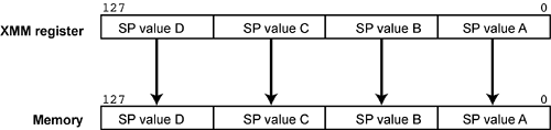
When this instruction is executed, the processor treats the line of memory space being written to as if it were the WC memory type (even though the MTRRs and the PTE or PDE selected by the linear address may designate it as WB memory). Executing this instruction has the following effects:
- The four, 32-bit SP FP numbers supplied from the specified XMM register are placed into the appropriate locations in one of the processor's WC buffers [WCB; see “Write-Combining (WC) Memory” on page 582 for more information] and the start address of the line is also latched into that WCB. The data will be written to memory at a later time when the WCB is written to memory over the FSB.
- Assuming that the memory type is WB, the line is not fetched from memory, so none of the disadvantages cited in Table 31-6 on page 777 are experienced.
- The processor performs a lookup in its internal caches and, if the line is present in the cache, it is evicted from the cache.
The MOVNTQ Instruction
Refer to Figure 31-9 on page 782. This instruction is a Store Qword Using a Non-Temporal Hint. When executed, it moves eight bytes of data from the specified MMX register into memory. When this instruction is executed, the processor treats the line of memory space being written to as if it were the WC memory type (even though the MTRRs and the PTE or PDE selected by the linear address may designate it as WB memory). Executing this instruction has the following effects:
- The eight bytes from the specified MMX register are placed into the appropriate locations in one of the processor's WC buffers [WCB; see “Write-Combining (WC) Memory” on page 582 for more information] and the start address of the line is also latched into that WCB. The data will be written to memory at a later time when the WCB is written to memory using the FSB.
- Assuming that the memory type is WB, the line is not fetched from memory, so none of the disadvantages cited in Table 31-6 on page 777 are experienced.
- The processor performs a lookup in its internal caches and, if the line is present in the cache, it is evicted from the cache.

The MASKMOVQ Instruction
Refer to Figure 31-10 on page 783. When executed, this instruction uses the bit mask specified in one MMX register to determine which of the eight bytes in another MMX register are to be written to memory. Bit 7 in each byte of the specified MMX mask register indicates whether the corresponding data byte from the other MMX register will be written to memory (1 = write the byte to memory; 0 = do not write it to memory). The memory address is specified in the DS:DI (if executing in 16-bit mode) or the DS:EDI register pair (if executing in 32-bit mode).

As mentioned in “Some Questions Regarding Documentation” on page 778, the author has some doubt as to whether or not this is a non-temporal store, but the following description assumes that it is:
- The specified bytes from the source MMX register are placed into the appropriate locations in one of the processor's WC buffers [WCB; see “Write-Combining (WC) Memory” on page 582 for more information] and the start address of the line is also latched into that WCB. The data will be written to memory at a later time when the WCB is written to memory over the FSB.
- Assuming that the memory type is WB, the line is not fetched from memory, so none of the disadvantages cited in Table 31-6 on page 777 are experienced.
- The processor performs a lookup in its internal caches and, if the line is present in the cache, it is evicted from the cache.
Also refer to “The Masked Move Operation” on page 788.
Ensuring Delivery of Writes Before Proceeding
An Example Scenario
Consider a scenario with the following assumptions:
The ports that are used to control and check the status of a graphics adapter have been implemented as memory-mapped IO ports. In other words:
- The status of the adapter is checked by performing an memory read from its status register.
- Parameters are supplied to the adapter by performing memory writes to its parameter registers.
- Commands are issued to the adapter by performing memory writes to its command port.
Data to be displayed by the adapter is written into its display frame buffer by performing memory writes to locations within the buffer.
Assume that the memory area within which the memory-mapped IO ports are located is defined as the UC or WC memory type.
In the device driver for the graphics adapter, a series of memory writes are performed to write a number of parameters into the adapter's parameter registers.
A memory write is then performed to the adapter's command register to change the adapter's screen resolution.
Since the memory type assigned to the adapter's memory-mapped IO register set is either UC or WC, the memory writes that were just performed to the parameter and command registers have not yet been performed on the FSB. Rather, they are buffered up either in the processor's internal PWBs (if the memory range is defined as the UC memory type), or WCBs (if the memory range is defined as the WC memory type). The parameters and the command have therefore not yet been received by the graphics adapter.
Now assume that to ensure proper operation of the driver, it is imperative that the adapter receive the parameters and the command before subsequent memory writes in the program are performed.
The SFENCE Instruction
When the SFENCE instruction is placed in a program's flow (see Figure 31-11 on page 785), the processor core treats it as a fence (i.e., a barrier) in the program flow. The core is not permitted to execute any stores that lie beneath the fence until the write data associated with all stores above the fence have been flushed from the processor WCBs (for writes to WC memory) and PWBs (for writes to UC, WP, or WT memory) to external memory over the processor's FSB—in other words, until memory has been brought up-to-date (i.e., it's been synchronized) vis a vis all processor memory updates.
Figure 31-11. Stores to WC Memory Are Posted in the WCBs

The core may, however, execute any non-store μops that lie beneath the SFENCE instruction before all of the previously-posted writes are dumped to memory.
As shown in Figure 31-11 on page 785, when a store to WC memory is executed, the processor posts the write data in one of its WCBs. The data is not written to memory until sometime later when the WCBs and PWBs are flushed to external memory over the FSB.
As shown in Figure 31-12 on page 786, when a store to WB memory is executed and the target line is already in the cache, the processor writes the data into the cache line and marks the line as Modified (if it wasn't marked so already). If the line was not already in the cache, the processor performs a Memory Read and Invalidate transaction on the FSB to obtain the line. The line is then placed in the cache, is written to and is marked Modified. It should be noted that the memory write data is not written to memory.
Figure 31-12. Stores to WB Memory Create Modified Cache Lines

As shown in Figure 31-13 on page 786, although the processor core can execute non-store μops that reside beneath the fence, it cannot execute any stores beneath the fence until the processor has dumped all of the memory writes queued up in its PWBs and WCBs to the FSB. Then and only then is the core permitted to execute any stores beneath the fence.
Figure 31-13. SFENCE Blocks the Core from Executing Downstream Stores

See Figure 31-14 on page 787. If, after the SFENCE has caused the buffer flush, another entity in the system (e.g., another processor) attempts to read data from any of the WC or UC memory locations that were written to, the data is sourced from memory (which has received the updates). If another entity in the system attempts to read data from any of the WB memory locations that were written to, it is snooped in this processor's caches and results in a hit on a modified line. In the Snoop Phase of the other entity's memory access the processor indicates a hit on a modified line (i.e., it asserts HITM# to other entity) and supplies the modified line to the other entity in the transaction's Data Phase.
Figure 31-14. Core Can Execute Downstream Stores After Buffers Are Flushed

Elimination of Mispredicted Branches
Background
As described earlier in the book (see “Elimination of Conditional Branches” on page 527), misprediction of conditional branch instructions causes a deep performance dip (because the entire instruction pipeline must be flushed). Of special concern are conditional branch instructions wherein the branch decision is based on unpredictable data (e.g., based on the state of visual data being received from a video source). MMX, SSE and, starting with the Pentium® 4, SSE2 all include instructions that were included specifically to eliminate (wherever possible) conditional branches that are based on unpredictable, random data comparisons.
SSE Misprediction Enhancements
Comparisons and Bit Masks
The SP FP comparison instruction (CMP) is similar to pre-existent MMX instructions (i.e., PCMPEQ, PCMPGT) in that it produces a mask value of all 1's (true) or all 0's (false) for each packed FP value, depending upon result of the comparison. The resultant masks can then be used with subsequent logic operations (e.g., AND, ANDN, OR, XOR) to perform conditional moves (thereby eliminating comparisons followed by conditional branches). Additionally, four mask bits (the msb of each mask) can be moved to an integer register using the MOVMSKPS/PMOVMSKB instructions. These instructions eliminate data-dependent branching, such as the clip extent and front/back-face culling checks in 3D geometry.
Min/Max Determination
Another important conditional usage model involves finding the maximum or minimum of two values (either packed or scalar values). While this can be accomplished as described in the previous paragraph, the MAX/MIN and PMIN/PMAX instructions accomplish it using a single instruction. It is accomplished by using the carry bit produced by the comparison subtraction (performed to determine the MIN or MAX value of the two) to select which source to forward to a destination. In 3D geometry and rasterization applications, color clamping is an example that benefits from the use of MINPS/PMIN. In addition, many speech recognition engines use the evaluation of a Hidden-Markov Model (HMM), and this function comprises upwards of 80% of execution time. The PMIN instruction improves the kernel performance by 33%, yielding a 19% application gain (these numbers are from Intel® documentation).
The Masked Move Operation
“The MASKMOVQ Instruction” on page 782 described the MASKMOVQ instruction. Using this instruction to conditionally move bytes into memory improves performance when compared to using conditional moves or conditional branches (the other methods inject more μops into the instruction pipeline, and using a conditional branch raises the possibility of branch mispredictions and the resultant performance penalty).
Reciprocal and Reciprocal Square Root Operations
Many basic operations in geometry involves performing divisions and computing square roots:
Example geometry operations wherein a division must be performed:
- Transformation frequently requires dividing each radix's x, y, z coordinates by the radix's w (perspective) coordinate.
- The specular lighting procedure includes a power function. This can be emulated using an approximation function that performs a division.
Normalization is a common geometry operation requiring the following calculation of the reciprocal of the square root of a value (1 ÷ the square-root of a value).
In order to provide an efficient method for handling these cases, SSE includes the following two approximation instructions:
The processor design implements these instructions using hardware lookup tables. While they are inherently less precise (only 12 bits of mantissa versus 24 for the full IEEE-compliant DIV and SQRT), they execute much faster than the full precision versions. If greater precision is required, these instructions can be used with a single Newton-Raphson (N-R) iteration to achieve almost the same precision as the IEEE instructions (yielding approximately 22 bits of mantissa). This N-R iteration for the reciprocal operation involves two multiplies and a subtraction, so it still executes more quickly than the IEEE instructions. When used in a basic geometry pipeline, these instructions can improve overall performance on the order of 15%.
MPEG-2 Motion Compensation
Motion compensation is the process of reconstructing each image frame in the output picture stream by interpolating between the pixels that comprise two key image frames. The interpolation consists of averaging the pixels from a macroblock in a frame with the pixels from the same respective macroblock in the next frame. A macroblock consists of a 16 x 16 pixel unit within a frame. The MPEG-2 specification requires that the resultant average must be rounded to the nearest integer (and values that fall exactly at the half way value must be rounded away from zero). This requires that the averaging operation have nine bits of precision.
SIMD instructions in the MMX instruction set provide either 8 or 16 bits of precision. Using the MMX SIMD instructions that operate on packed bytes (rather than packed words) increases the throughput.
While the SSE PAVG instruction performs a 9-bit accurate averaging operation on packed bytes, the PAVGW instruction operates on packed words and provides higher accuracy for applications that accumulate a result using several computation instructions.
At the time that SSE was introduced (with the advent of the Pentium® III), the Motion Compensation element of a DVD player application executed on a Pentium® II-based system operating at a core speed of 266MHz spent about as much time accessing memory as it did executing.
Implementing the Motion Compensation function using the SSE PAVG instruction enabled a 25% kernel speedup (by Intel®'s measurements), and a 4% to 6% speedup at the application level (depending on the video clip chosen). Intel® estimated that the application-level gain could increase to 10% for higher resolution HDTV digital television formats.
Optimizing 3D Rasterization Performance
Intel®'s investigation into operations that were not optimized in the 3D realm revealed that MMX's lack of an unsigned multiply operation resulted in inefficient 3D rasterization performance. 3D rasterization is accomplished by operating on unsigned pixel data, and the MMX PMULHW instruction operates only on signed data. Providing an unsigned PMULHUW in the SSE instruction set eliminated the fix-up overhead that was required when using the signed MMX operation, yielding an application-level performance gain of 8%-10%.
Optimizing Motion-Estimation Performance
During the video encode process, an estimated 40%-70% of the execution time is spent in the Motion-Estimation function. This stage of the encode pipeline compares a sub block of the current frame with sub blocks in the same relative position of the previous and next frames in order to find the best match. The compressed output stream only includes a vector representing the position of the two sub blocks and the residual difference between the two sub blocks.
Two common comparison metrics are used in motion-estimation:
SSD could be implemented using an unsigned multiply and accumulate operation (byte to word), but the accumulation range requires 24 bits of precision, (which does not map neatly to a general purpose data-type). The SSE PSADBW (Compute Sum of Absolute Differences) instruction performs a SIMD operation on eight bytes simultaneously (but the accumulation does not exceed a 16-bit word). This SSE instruction replaces approximately seven MMX instructions in the motion-estimation's inner loop (because MMX does not support unsigned byte operations; they must be emulated by zero extension to words and the use of word operations). Intel® estimates the use of the PSADBW instruction can increase the performance of the motion-estimation function by a factor of two.
Summary of the SSE Instruction Set
Table 31-7 on page 791 provides a summary of the instructions introduced in the SSE instruction set. The following is a key to the instruction suffixes found the table:
ss = scalar SP FP.
ps = packed SP FP.
pi = packed dword integers.
si = signed dword integer.
| Data Movement | Arithmetic | Logical | Comparison | Shuffle and Unpack | Conversion | 64-bit SIMD Integer | MXCSR State Management | Cacheability and Memory Ordering Related |
|---|---|---|---|---|---|---|---|---|
| movaps | addps | andps | cmpps | shufps | cvtpi2ps | pavgb | ldmxcsr | movntq |
| movups | addss | andnps | cmpss | unpckhps | cvtsi2ss | pavgw | stmxcsr | movntps |
| movss | mulps | orps | comiss | unpcklps | cvtps2pi | pextrw | maskmovq | |
| movlps | mulss | xorps | ucomiss | cvttps2pi | pinsrw | prefetch | ||
| movhps | divps | cvtss2si | pmaxub | SFENCE | ||||
| movlhps | divss | cvttss2si | pminub | |||||
| movhlps | rcpps | pmaxsw | ||||||
| movmskps | rcpss | pminsw | ||||||
| sqrtps | pmovmskb | |||||||
| sqrtss | pmulhuw | |||||||
| rsqrtps | psadbw | |||||||
| rsqrtss | pshufw | |||||||
| maxps | ||||||||
| maxss | ||||||||
| minps | ||||||||
| minss | ||||||||
| subps | ||||||||
| subss |
SSE Alignment Checking
Except in the following cases, the address of a 128-bit packed memory operand must be aligned on a 16-byte boundary:
Scalar instructions that use a 32-bit memory operand are not subject to alignment requirements.
The MOVUPS (Move Unaligned Packed SP FP) instruction performs the same operations as the MOVAPS instruction, except that 16-byte alignment of a memory address is not required.
The SIMD FP Exception
The SIMD FP exception (exception 19) was added with the advent of the Pentium® III processor (see “SIMD Floating-Point Exception (19)” on page 326).
SIMD FP exceptions are generated independently from the x87 FP exceptions. Generation of an SSE SIMD FP exception does not result in the assertion of the processor's FERR# output pin (regardless of the CR0[NE] setting), and the state of the processor's IGNNE# input pin has no effect on the SSE SIMD FP logic. See “FPU Added On-Die” on page 432 for more information.
SSE Setup
To set up the SSE extensions (and SSE2 extensions starting with the Pentium® 4) for use by application programs, the OS must perform the following steps:
1. | |
2. | |
3. | |
4. |
The OSFXSR and OSXMMEXCPT bits in CR4 must be set by the OS because the processor has no other way of detecting OS support for the FXSAVE and FXRSTOR instructions or for handling SIMD FP exceptions.