
The IO APIC
The Purpose of the IO APIC
When a device adapter issues an interrupt request to a processor, it is issued in one of two forms:
By asserting one of the IRQ signal lines.
By performing an MSI write transaction in the form of a memory-mapped IO write [see “Message Signaled Interrupts (MSI)” on page 1584].
The IO APIC is incorporated within the chipset and its inputs are connected to the IRQ lines (and possibly to the SMI# signal line). When a device adapter asserts an IRQ line or when the system board logic asserts the SMI# signal, the IO APIC converts this into an interrupt message and transmits it to the processors either over the 3-wire APIC bus (for the Pentium® and P6 processors families; see Figure 61-28 on page 1568), or the FSB (for the Pentium® 4 family processors; see Figure 61-29 on page 1569).
Figure 61-28. The IO APIC and Pentium® or P6 Processors

Figure 61-29. The IO APIC and Pentium® 4 Family Processors

The number of IRQ inputs implemented on an IO APIC as design-specific, but 24 is a very common number. For each of the IRQ inputs (and the SMI# input, if the IO APIC has one), the IO APIC implements a register that is programmed by the BIOS or the OS with:
Information regarding the IRQ signal's characteristics (whether an interrupt is signaled by the rising-edge of the signal or by a static voltage level, and if it's by a static voltage level, whether a static high or low should be recognized as a valid interrupt).
Information necessary to compose the interrupt message to be sent to the processors.
This register set is referred to as the Redirection Table, or RT.
As mentioned at the beginning of this section, device adapters may also generate an interrupt request by performing an MSI write transaction in the form of a memory-mapped IO write. This memory write transaction targets one of the following:
The IO APIC implements a special memory-mapped IO port dedicated to the receipt of MSI writes from device adapters. The OS may program a device adapter's MSI register set with the address of this port as well as the data to be written to it. When the device generates an interrupt request, it does so by generating a memory write to the special IO APIC port. Upon receipt of such a message, the IO APIC generates an interrupt message on the 3-wire APIC bus (for the Pentium® and P6 processors), or on the FSB (for the Pentium® 4 processor family).
In a Pentium® 4-based system, the OS may program a device adapter's MSI register set with the address of the processors' Local APICs as well as the data to be written to the Local APICs. When the device generates an interrupt request, it does so by generating a memory write to the Local APIC address. Upon receipt of such a message, the IO APIC is bypassed. The ICH (see Figure 61-29 on page 1569) passes the MSI write to the MCH and the MCH passes it to the FSB without modification.
Overview of an Edge-Triggered Interrupt Delivery
This overview makes the following assumptions:
The device adapter is connected to the IO APIC's input number 3 (RT register 0 is associated with input 1, RT register 1 is associated with input 1, etc.).
The device adapter issues an interrupt request by generating a low-to-high transition on its IRQ signal line.
Input 3 has been programmed (via RT register 2 in the IO APIC) as follows:
- It is an edge-triggered input.
- It specifies Physical Destination Mode and targets the Local APIC that has been assigned a Local APIC ID of 23h.
- It uses Fixed Delivery Mode and specifies a user-defined interrupt vector of 20h.
It also assumes that the system is based on Pentium® 4 family processors (see Figure 61-5 on page 1506).
The device adapter issues an interrupt request by generating a low-to-high transition on its IRQ signal line.
On detection of the low-to-high transition (i.e., the positive-going edge) on input 3, the IO APIC sets the Delivery Status bit = 1 in RT register 2, indicating that the message has not yet been accepted by the processors.
Using the information programmed into RT register 2, the IO APIC formulates the interrupt message as a memory write to the Local APICs within the processors on the FSB.
The ICH forwards the memory write across the Hub Link to the MCH.
The MCH determines from the memory address (i.e., the address of the Local APICs) that the memory write should be forwarded to the FSB.
The MCH asserts the BPRI# signal on the FSB to request ownership of the Request Phase signal group.
Upon attaining ownership of the Request Phase signal group, the MCH initiates the memory write transaction that represents the interrupt message.
All of the processors latch the transaction request, decode the target memory address and deliver the interrupt message to their respective Local APICs.
This example assumes that the message specifies Physical Destination Mode targeting Local APIC 23h. Local APIC 23h recognizes that it is the target of the message, while the other Local APICs ignore the message.
Local APIC 23h sets the bit in its Interrupt Request Register (IRR) that is selected by the user-defined vector delivered in the message (20h). In this example, its sets bit 3210 in the IRR to one to indicate that vector 20h (3210) has an interrupt request pending delivery to the processor core.
Having accepted the message, the processor allows the FSB memory write transaction to end normally. The Local APIC may have previously accepted earlier messages with a vector of 20h and bit 20 may already be set to one in the IRR. In this case, the new message is accepted and IRR bit 20 remains set to one.
Upon receipt of the Normal Response to the memory write transaction, the MCH sends an acknowledgement of successful message transmission to the ICH over the Hub Link interface.
The ICH clears the Delivery Status bit in RT entry 2 to 0. The IO APIC cannot recognize another edge-triggered interrupt on input 3 until this bit has been cleared.
Within the target processor, the Local APIC eventually dispatches user-define interrupt 20h to the processor core (see “The Priority Amongst the User-Defined Interrupts” on page 1519). When it does so, IRR bit 3210 is cleared and ISR bit 3210 is set to indicate that the interrupt is now being serviced.
The interrupt handler is executed. Towards the end of the handler, the handler performs a memory write to the Local APIC's EOI (End-of-Interrupt) register. This causes the Local APIC to clear ISR bit 3210.
Overview of a Level-Sensitive Interrupt Delivery
This overview makes the following assumptions:
The device adapter is connected to the IO APIC's input number 3 (RT register 0 is associated with input 1, RT register 1 is associated with input 1, etc.).
The device adapter issues an interrupt request by driving input 3 low and it will continue to drive it low until it has been serviced by the interrupt handler within its device driver.
Input 3 has been programmed (via RT register 2 in the IO APIC) as follows:
- It is a level-sensitive input.
- It recognizes an electrical low as a valid interrupt request.
- It specifies Physical Destination Mode and targets the Local APIC that has been assigned a Local APIC ID of 23h.
- It uses Fixed Delivery Mode and specifies a user-defined interrupt vector of 20h.
It also assumes that the system is based on Pentium® 4 family processors (see Figure 61-5 on page 1506).
The device adapter issues an interrupt request by driving a low on its IRQ signal line.
On detection of the electrical low on input 3, the IO APIC sets the Remote IRR bit (Interrupt Request Register) and the Delivery Status bit = 1 in RT register 2:
- Setting the Remote IRR bit in RT register 2 indicates a request has been received, but that it has not yet been serviced by the interrupt handler.
- Setting the Delivery Status bit in RT register 2 indicates that the message has not yet been accepted by the processors.
Using the information programmed into RT register 2, the IO APIC formulates the interrupt message as a memory write to the Local APICs within the processors on the FSB.
The ICH forwards the memory write across the Hub Link interface to the MCH.
The MCH determines from the memory address (i.e., the address of the Local APICs) that the memory write should be forwarded to the FSB.
The MCH asserts the BPRI# signal on the FSB to request ownership of the Request Phase signal group.
Upon attaining ownership of the Request Phase signal group, the MCH initiates the memory write transaction that represents the interrupt message.
All of the processors latch the transaction request, decode the target memory address and deliver the interrupt message to their respective Local APICs.
This example assumes that the message specifies Physical Destination Mode targeting Local APIC 23h. Local APIC 23h recognizes that it is the target of the message, while the other Local APICs ignore the message.
Local APIC 23h sets the bit in its Interrupt Request Register (IRR) that is selected by the user-defined vector delivered in the message (20h). In this example, its sets bit 3210 in the IRR to one to indicate that vector 20h (3210) has an interrupt request pending delivery to the processor core.
Having accepted the message, the processor allows the FSB memory write transaction to end normally. The Local APIC may have previously accepted earlier messages with a vector of 20h and bit 20 may already be set to one in the IRR. In this case, the new message is accepted and IRR bit 20 remains set to one.
Upon receipt of the Normal Response to the memory write transaction, the MCH sends an acknowledgement of successful message transmission to the ICH over the Hub Link interface.
The IO APIC clears the Delivery Status bit to 0. The IO APIC cannot recognize another level-sensitive interrupt on input 3 until this bit has been cleared.
The IO APIC sets the Remote IRR bit in RT register 2 to indicate that the interrupt has been accepted by the processor but has not yet been serviced. The IO APIC cannot accept another interrupt request on input 3 until this bit is cleared by the Local APIC.
Within the target processor, the Local APIC eventually dispatches user-define interrupt 20h to the processor core (see “The Priority Amongst the User-Defined Interrupts” on page 1519). When it does so, IRR bit 3210 is cleared and ISR bit 3210 is set to indicate the interrupt is now being serviced.
The interrupt handler is executed. Towards the end of the handler, the handler performs a memory write to the Local APIC's EOI (End-of-Interrupt) register. This causes the Local APIC to clear ISR bit 3210.
When an interrupt handler writes to the Local APIC's EOI register to clear a level-sensitive request, the Local APIC not only clears the ISR bit related to the interrupt, but also performs a memory write transaction on the FSB to write the interrupt vector (20h in this case) to the IO APIC's EOI register.
Upon receipt of the write to its EOI register, the IO APIC compares the vector in the EOI register to the vectors programmed into the RT registers for all of its inputs. The input with the matching vector (20h in this case) clears the Remote IRR bit in its respective RT entry to 0, thereby reenabling recognition of a low level on input 2 as another request.
Additional information can be found in “The EOI Register” on page 1578.
The IO APIC Register Set
The IO APIC Register Set Base Address
The default base address of the IO APIC's memory-mapped IO register set is FEC00000h. Depending on the chipset, the base address may or may not be programmable. If it is programmable, the register that is used to reprogram the base address is typically called the APICBASE register and the register address is chipset design-specific.
The IO APIC Register Set
The IO APIC's register set consists of the registers listed in Table 61-7 on page 1574. While the Index Register, the Data Register, the IRQ Pin Assertion Register and the EOI are directly-addressable, the indirectly-addressable registers are accessed by first writing the 8-bit Index value of the desired register into the Index Register. This selects the desired register. A subsequent read from or write to the Data Register accesses the desired register.
| Register | Start Address | Width (in bits) | R/W | Description |
|---|---|---|---|---|
| Directly-Addressable Registers | ||||
| Index Register | FEC00000h | 8 | R/W | Name: IND. To access any of the indirectly-accessed registers, the programmer first writes the register's index value into this register. This selects the desired register. A subsequent read from or write to the Data Register accesses the desired register. |
| Data Register | FEC00010h | 32 | R/W | |
| IRQ Pin Assertion Register | FEC00020h | 32 | WO | Name: IRQPA. This is a special, memory-mapped IO write register to which device adapters can perform an MSI write to issue an interrupt request. See “The IRQ Pin Assertion Register” on page 1577. |
| EOI Register | FEC00040h | 32 | WO | Name: EOIR. The End-of-Interrupt register is only applicable if any of the IO APIC's inputs are designated as level-sensitive (rather than positive edge-triggered) inputs. At the end of the interrupt handler routine associated with a level-sensitive, user-defined interrupt, the programmer performs a write to the EOI register in the Local APIC. This causes the Local APIC to clear the ISR bit (In-Service Register) associated with this interrupt. In addition, the Local APIC automatically issues an EOI message to the IO APIC's EOI register (in the form of a memory write containing the vector to be cleared). In response, the IO APIC clears the Remote IRR bit in the RT entry that contains that interrupt vector. See “The EOI Register” on page 1578. |
| Indirectly-Accessed Registers (accesses to these registers must be 32-bit accesses) | ||||
| Identification Register | Index 00h | 32 | R/W | Name: ID. This register contains the unique APIC ID assigned to the IO APIC module. See “The ID Register” on page 1581. |
| Version Register | Index 01h | 32 | RO | Name: VER. This read-only register contains the following information:
|
| Reserved | Index 02h-0Fh | - | RO | |
| Redirection Table Register 0 | Index 10h-11h | 64 | R/W RO | Name: REDIR_TBL0. This is the first entry in the Redirection Table and is associated with IRQ input 1. See “The Redirection Table Register Set” on page 1581. |
| Redirection Table Register 1 | Index 12h-13h | 64 | R/W RO | Name: REDIR_TBL1. This is the second entry in the Redirection Table and is associated with IRQ input 2. |
| Redirection Table Register n | --- | 64 | R/W RO | Name: REDIR_TBLn. This is the nth entry in the Redirection Table and is associated with IRQ input n+1. The number of table entries (and input pins) is IO APIC design-specific. |
| Reserved | Index values through FFh | - | RO | |
The IRQ Pin Assertion Register
This is a special, write-only, memory-mapped IO port (at memory address FEC00020h) to which device adapters can perform an MSI write to deliver an interrupt request to the IO APIC (in the form of a virtual IRQ pin assertion). To generate an interrupt request, the device adapter writes a 32-bit value into this register (see Figure 61-30 on page 1577). Register bits [4:0] contain the IRQ number associated with this interrupt. Since currently-available IO APICs only implement 24 IRQ inputs, the only valid values are 0–23. The IO APIC ignores bits [31:5]. To provide for future expansion, device adapters must always write a value of 0 into bits [31:5].
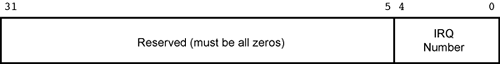
On receipt of an IRQ number in this register, the IO APIC uses the RT entry associated with the specified IRQ to format an interrupt message to send to the processors (see “The Redirection Table Register Set” on page 1581 for more information). It should be noted that the Intel ICH5 Data Sheet specifies that the selected IRQ pin's RT register must be programmed as an edge-triggered interrupt.
The EOI Register
Non-Shareable IRQ Lines
In the early PC days, very few IRQ lines were available to the designers of device adapters. This was further complicated by the type of signaling device adapters used to signal an interrupt request. The 8259A interrupt controller only recognized the positive-edge (i.e., the rising-edge) of the IRQ signal as representing a valid request for service. Two or more adapters could not share an IRQ because each would drive the signal line high to indicate a request for service.
Shareable IRQ Lines
Later, the PCI spec defined active-low, level-sensitive IRQ lines that could be shared among multiple device adapters. Refer to Figure 61-32 on page 1580. Each shareable IRQ line has a pull-up resistor that maintains the IRQ line in the deasserted (electrically-high) state when no adapters are driving it low.

When one or more adapters require service, each of them gates a logic low onto the signal line. A logic low on a shared IRQ line indicates that one or more adapters require serving. When the interrupt controller detects a low on a shared input, it generates an interrupt to the processor and supplies it with the vector associated with that IRQ line. The processor uses the vector to index into the IDT and jumps to the interrupt handler pointed to by the selected entry.
Linked List of Interrupt Handlers
That raises a question: Which adapter's interrupt handler does the selected IDT entry point to? Earlier in time, the OS loaded the device drivers associated with the installed devices. When a driver is loaded into memory by the OS, the OS the calls the driver's initialization code entry point to finish the setup of the device. As part of this process, assuming that the device uses a shared IRQ line, the driver's initialization code reads the pointer already stored in the respective IDT entry and stores that pointer within the body of the driver. It then writes the pointer to its own interrupt handler into this IDT entry. The next driver whose adapter uses the same IRQ line is loaded by the OS and its initialization code is called. It reads the IDT entry (which contains the pointer to the previously-loaded driver's interrupt handler) and saves that pointer in the body of its driver. It then replaces the IDT entry with the pointer to its own interrupt handler. A linked-list of interrupt handlers that share this vector is being dynamically created.
How It Works
Refer to Figure 61-32 on page 1580 (ignore the Interrupt Router; it's chipset-specific and permits the OS to choose to which of the interrupt controller's inputs the signal is routed) and assume that both adapters generate an interrupt by placing a low on the shared IRQ line. The IO APIC (labelled “interrupt Controller” in the figure) sets a bit to register the fact that an adapter attached to this line needs to be serviced. The IO APIC formulates an interrupt message and sends it to the processor. On receipt of the message, the Local APIC passes the interrupt vector to the processor. The processor uses it to index into the IDT and jumps to the interrupt handler associated with the driver that “hooked” that IDT entry last during the driver load process. That handler executes and the first thing the handler does is to read the Interrupt Pending bit from an adapter-specific port to determine if the adapter is really generating an interrupt. Assuming the bit is set, the body of the handler is executed, thereby servicing the adapter associated with that handler. The act of servicing the adapter causes the adapter to clear its Interrupt Pending bit and to cease driving the IRQ line low. However, the line remains low if another adapter that has not yet been serviced is still driving it low.
Although servicing the first adapter cleared the request from the adapter's perspective, the IO APIC doesn't know that it has been serviced. At the end of the interrupt handler, the programmer performs a memory-mapped IO write to the Local APIC's EOI register. This causes the Local APIC to clear the IRR bit associated with that vector thereby signifying that the interrupt has completed servicing. If the interrupt was defined as an active-low, level-sensitive interrupt, however, the Local APIC must also inform the IO APIC that the interrupt has completed servicing. It does this by automatically performing a memory-mapped IO write to the IO APIC's (write-only) EOI register (see Figure 61-31 on page 1580) and the data written is the vector for the interrupt. Upon receipt of the write to the EOI register, the IO APIC uses the vector number supplied in the EOI write and clears the Remote IRR bit in the RT entry associated with the IRQ line. This clears the bit, signifying the fact that the first adapter has been served.

If the IRQ line is still low, however, the IO APIC sets the RT entry's Remote IRR bit again and generates another interrupt message to the processor with the same interrupt vector. The process just described is repeated until all pending requests on that IRQ line have been serviced and the pull-up resistor pulls the line to the deasserted state.
The ID Register
The OS writes the APIC ID for the IO APIC into this 32-bit read/write register.
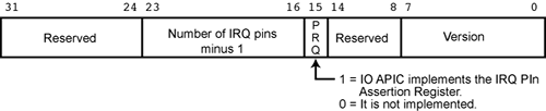
The Version Register
See Figure 61-33 on page 1581. This read-only register contains the following information:
The number of IRQ input pins implemented and therefore the number of entries in the Redirection Table (RT).
A bit that indicates whether or not the IO APIC implements the IRQ Pin Assertion Register.
The version number of the IO APIC implementation.
The Redirection Table Register Set
As mentioned earlier, the IO APIC implements a configuration register for each of the IRQ input pins implemented on the IO APIC (and the number of IRQ input pins is IO APIC design-specific). This register set is referred to as the Redirection Table, or RT. Each entry is 64-bits wide and has the format shown in Figure 61-34 on page 1582 and Table 61-8 on page 1582.

| Bit(s) | Description |
|---|---|
| 63:56 | Destination field. R/W.
|
| 55:48 | Reserved. |
| 47:17 | Reserved. |
| 16 | Mask bit. R/W.
|
| 15 | Trigger Mode. R/W. This field indicates the type of signal on the interrupt pin that is recognized as a valid interrupt request: |
| 14 | Remote IRR (Interrupt Request Register). R/W. This bit only applies to level-sensitive interrupts. Its meaning is undefined for edge-triggered interrupts:
|
| 13 | Interrupt Input Pin Polarity. R/W. This bit only applies if this pin is defined as a level-sensitive interrupt. It specifies if a valid interrupt request is signified by an electrical low or high:
|
| 12 | Delivery Status. RO. Indicates the current status of the delivery of this interrupt: |
| 11 | Destination Mode. R/W. This field determines the interpretation of the Destination field:
|
| 10:8 | Delivery Mode. R/W. See Figure 61-34 on page 1582. |
| 7:0 | Vector. R/W. This field contains the user-defined interrupt vector associated with this pin. Valid values range between 10h and FEh. |
When an edge-triggered interrupt is detected, the respective RT entry's Delivery Status bit is set to one to indicate that the message has not yet been sent to the processor(s). Once the message has been sent, the Delivery Status bit is cleared and only then can the IO APIC recognize a new interrupt request on that input pin.
Interrupt Delivery Order Is Rotational
Unlike the Local APIC, the IO APIC does not implement a priority scheme to determine the order in which interrupt messages associated with each of its inputs are delivered to the processors. Rather, the IO APIC constantly rotates through its RT registers and, if the Delivery Status bit in the currently-selected register is set to one, it sends the message associated with that RT to the processors.