
Store μops
Store instructions are those that write the contents of a processor register to memory.
Stores Are Handled by the Store Buffers
“Background” on page 1070 introduced the Store Buffers.
Store instructions are executed in strict program order and are never executed speculatively. Figure 41-2 on page 1073 pictures the Store execution units:
On an integer store operation, the double-speed ALU on port 0 executes the Store Data μop. The Store Address execution unit on port 3 simultaneously executes the Store Address μop.
On a FP, SSE or SSE2 store operation, the FP Move execution unit on port 1 executes the Store Data μop. The Store Address execution unit on port 3 simultaneously executes the Store Address μop.

Stores to UC Memory
General
Refer to Figure 41-3 on page 1075. UC is one of the two uncacheable memory types (the other is the WC memory type). When a store to UC memory is executed, it is posted in the Store Buffer reserved for it in the Allocator stage. Stores to UC memory are also submitted to the L1 Data Cache, the L2 Cache, or the L3 Cache (if there is one). In the event of a cache hit, the line is evicted from the cache.
Figure 41-3. Stores to UC Memory

UC Store Buffer Draining
Any stores to UC memory will remain in the processor's Store Buffers until one of the events described in “Forcing a Buffer Drain” on page 1083 occurs. It should be noted that when another agent on the FSB initiates a memory transaction, it is not snooped in the processor's Store Buffers. Any updates that are sitting in the Store Buffers are therefore invisible to other bus agent. See “Sharing Access to a UC, WC, WP or WT Memory Region” on page 1085 for more information.
UC FSB Transactions
When a Store Buffer containing a store to UC memory is forwarded to the FSB Interface Unit, a Memory Data Write transaction with the following characteristics is performed on the FSB:
If the store writes between one and eight bytes into a single qword of memory space, the FSB transaction is performed as a single qword Memory Data Write with the appropriate Byte Enable signals asserted to indicate which bytes of the qword are being written to.
If a multi-byte store crosses a qword address boundary, the FSB Interface Unit performs two separate, single-qword Memory Data Writes with the appropriate Byte Enable signals asserted to indicate which bytes of each qword are being written to.
If a 64-bit register (an MMX register) is being stored to memory starting at an address divisible by eight, the FSB transaction is performed as a single-qword Memory Data Write with all eight of the Byte Enable signals asserted indicating that all of the bytes in the qword are being written to.
If a 128-bit register (an XMM register) is being stored to memory starting at an address divisible by 16, the FSB transaction is performed as a two qword Memory Data Write with all eight of the Byte Enable signals asserted. The two qwords are written in toggle mode transfer order (see “The Burst Transaction” on page 472).
Stores to WC Memory
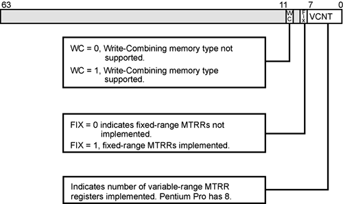
Determining if the WC Memory Type Is Supported
The programmer may determine whether or not a processor supports the WC (Write Combining) memory type by verifying that bit 10 is set to one in the IA32_MTRRCAP MSR (see Figure 41-4 on page 1076).
Figure 41-4. MTRRCAP MSR
The WC Memory Model
The WC memory type is well-suited to an area of memory (e.g., the video frame buffer) that has the following characteristics:
The processor does not cache from WC memory.
Speculative execution of loads from WC memory is permitted.
Stores to WC memory are deposited in the processor's Write Combining Buffers (WCBs).
It should be noted that when another agent on the FSB initiates a memory transaction, it is not snooped in the processor's Store Buffers or in its WCBs. Any updates that are sitting in the Store Buffers or WCBs are therefore invisible to other bus agent. See “Sharing Access to a UC, WC, WP or WT Memory Region” on page 1085 for more information.
Each WCB can hold one line (64 bytes of data).
As stores are performed to a line of WC memory space, the bytes are accumulated in the WCB assigned to record writes to that line of memory space.
A subsequent store to a location in a WCB can overwrite a byte that was deposited in that location by an earlier store to that location. In other words, multiple writes to the same location are collapsed so that the location reflects the last data byte written to that location.
When the WCBs are ultimately dumped to external memory over the FSB, data is not necessarily written to memory in the same order in which the earlier programmatic stores were executed. The device being written to must tolerate this type of behavior (i.e., it must function correctly). See “WCB FSB Transactions” on page 1080 for more information.
WCB Evolution
The size and number of WCBs implemented in a processor is design-specific:
The Pentium® Pro and Pentium® II implemented a single WCB which could hold up to one line of data (32 bytes). These processors did not automatically dump the WCB to memory when it became full.
The Pentium® III processor implemented four 32-byte buffers that did double-duty as cache line fill buffers (to handle cache misses) and as WCBs. The Pentium® III processors automatically dump a WCB to memory when it becomes full.
The Pentium® 4 family processor implement six, 64-byte WCBs, four of which are dedicated as WCBs, while other two can be used as WCB or for another special purpose (see “A Special Use of the WCBs” on page 1080). The Pentium® 4 family processors automatically dump a WCB to memory when it becomes full.
Filling the WCBs
Refer to Figure 41-5 on page 1078. When a store is performed to WC memory, the data is temporarily stored in the Store Buffer that was reserved for the store in the Allocator stage. As quickly as possible, the store is then forwarded to an available WCB.
Figure 41-5. Stores to WC Memory

If four of the six WCBs are currently in use (two of the six buffers may be temporarily unavailable to handle writes to WC memory; see “A Special Use of the WCBs” on page 1080) and additional stores are performed that store to WC lines other than those currently being handled by the four WCBs, the store buffers cannot be dumped to the WCBs and the Store Buffers begin to fill up. These buffers are a valuable resource and this will cause performance to degrade. No more stores can be executed until one or more of the WCBs are dumped to the L2 Cache or to external memory.
When the currently-executing program writes the first byte or bytes into a line of WC memory space, the next available 64-byte WCB memorizes the 64-byte aligned start address of the block the bytes are to be written to as well as the bytes to be written within the block. The WCB continues to accumulate additional WC stores to that line within the WCB until one of the following occurs (see “Draining the WCBs” on page 1079 for a more detailed explanation):
If and when the buffer becomes full, the WCB's contents are forwarded to the FSB Interface Unit and the processor automatically writes the line to memory as a burst transaction (see “WCB FSB Transactions” on page 1080).
When a synchronizing event occurs (see “Draining the WCBs” on page 1079).
When a SFENCE instruction is executed (see “The SFENCE Instruction” on page 1084).
When an MFENCE instruction is executed (see “The MFENCE Instruction” on page 1089.
Draining the WCBs
General
The WCBs continue to accumulate additional WC store data until one of the following occurs:
- If and when the buffer becomes full, the WCB's contents are forwarded to the FSB Interface Unit and the processor automatically writes the line to memory as a burst transaction (see “WCB FSB Transactions” on page 1080).
- The execution of the IN or OUT IO instructions.
- When a SFENCE instruction is executed (see “The SFENCE Instruction” on page 1084).
- When an MFENCE instruction is executed (see “The MFENCE Instruction” on page 1089.
- When the processor core sends an Interrupt Acknowledge to the 8259A interrupt controller.
- The execution of a locked Read/Modify/Write operation.
- When all of the WCBs are in use and another WC store is executed to a different line than those already recorded in the WCBs.
- When a serializing instruction is executed. See “Serializing Instructions” on page 1079.
- When the BINIT# signal is asserted (see the BINIT# entry in Table 55-1 on page 1314).
Serializing Instructions
The following instructions act as a fence in the program: the core is not permitted to execute any μops beyond the fence until all μops up to and including the fence instruction have completed execution and have been retired (note that this significantly reduces the processor's performance). In addition to serializing program execution, these instructions also cause the processor to dump all of its Store Buffers and WCBs to external memory before proceeding beyond the fence:
- The execution of WBINVD, INVD, WRMSR, or a move into CR0 when the state of the CD bit (Cache Disable) is altered, causes the execution of both threads on both logical processors to be serialized.
- The privileged serializing instructions: MOV to a Control Register, MOV to a Debug register, WRMSR, INVD, INVLPG, WBINVD, LGDT, LLDT, LIDT, and LTR.
- The non-privileged serializing instructions: CPUID, IRET, and RSM.
- The non-privileged memory ordering instructions:
- The SFENCE (see “The SFENCE Instruction” on page 1084) and MFENCE (see “The MFENCE Instruction” on page 1089) instructions cause the processor to drain all of its Store Buffers and WCBs to memory before executing any store μops beyond the fence. These instructions have a less damaging effect on performance because the processor is permitted to execute non-store μops (and, in the case of the MFENCE instruction, non-load μops) beyond the fence before the buffer draining has been completed.
A Special Use of the WCBs
Two of the WCBs can be used to expedite matters should a store to WB memory result in an L1 Data Cache miss. Refer to “Stores to WB Memory” on page 1086 for more information.
The WCBs and Hyper-Threading
Refer to “WCB Usage” on page 1004.
WCB FSB Transactions
The conditions under which the WCBs are drained to system memory were described in “Draining the WCBs” on page 1079.
A full WCB is written to system memory using a 64-byte burst Memory Data Write transaction. The start address can be any of the qword addresses within the line.
If a WCB is only partially full, the processor can write it to memory in one of the following ways:
- Any qword in the WCB that will not update all bytes in the qword is written to memory using a single qword Memory Write transaction (with only the appropriate Byte Enables asserted).
- If two successive qwords in the WCB will update all bytes within both qwords, the processor could perform a two-qword Memory Write transaction (and the two qwords are written to memory in toggle mode transfer order; see “The Burst Transaction” on page 472).
- If four successive qwords in the WCB (starting at an address divisible by 32) will update all bytes within the qwords, the processor could perform a four-qword Memory Write transaction (and the four qwords are written to memory in toggle mode transfer order; see “The Burst Transaction” on page 472).
The order in which the WCBs are written to memory is processor design-specific.
The order in which the qwords within a WCB are written to memory is processor design-specific.
Stores to WP Memory
General
When a store is performed to cacheable Write-Through memory, it is submitted to the caches and, in the event of a hit, the line is evicted from the cache (it should be noted, however, that this behavior is processor design-specific). The store is absorbed into the Store Buffer reserved for its use in the Allocator stage.
WP Store Buffer Draining
Any stores to WP memory will remain in the processor's Store Buffers until one of the events described in “Forcing a Buffer Drain” on page 1083 occurs. It should be noted that, when another agent on the FSB initiates a memory transaction, it is not snooped in the processor's Store Buffers. Any updates that are sitting in the Store Buffers are therefore invisible to other bus agent. See “Sharing Access to a UC, WC, WP or WT Memory Region” on page 1085 for more information.
WP FSB Transactions
When a Store Buffer containing a store to WP memory is forwarded to the FSB Interface Unit, a Memory Data Write transaction with the following characteristics is performed on the FSB:
If the store writes between one and eight bytes into a single qword of memory space, the FSB transaction is performed as a single qword Memory Data Write with the appropriate Byte Enable signals asserted to indicate which bytes of the qword are being written to.
If a multi-byte store crosses a qword address boundary, the FSB Interface Unit performs two, separate single qword Memory Data Writes with the appropriate Byte Enable signals asserted to indicate which bytes of each qword are being written to.
If a 64-bit register (an MMX register) is being stored to memory starting at an address divisible by eight, the FSB transaction is performed as a single qword Memory Data Write with all eight of the Byte Enable signals asserted indicating that all of the bytes in the qword are being written to.
If a 128-bit register (an XMM register) is being stored to memory starting at an address divisible by 16, the FSB transaction is performed as a two qword Memory Data Write with all eight of the Byte Enable signals asserted. The two qwords are written in toggle mode transfer order (see “The Burst Transaction” on page 472).
Stores to WT Memory
General
Refer to Figure 41-6 on page 1083. When a store to cacheable, Write-Through memory is executed. The store is posted in the Store Buffer that was reserved for its use in the Allocator stage. In addition, the store is submitted to the L1 Data Cache for a lookup. There are several possibilities:
If the store hits on the Data Cache, the line in the cache is updated, but it remains in the S state (which means the line is valid).
If the store misses the Data Cache, it is forwarded to the L2 Cache and a lookup is performed:
- If it hits on a line in the L2 Cache, the line is updated, but it remains in the S state (which means the line is valid).
- If it misses on the L2 Cache and there is no L3 Cache, no further action is taken.
- If it misses on the L2 Cache and there is an L3 Cache, the store is submitted to the L3 Cache. If it misses on the L3 cache, no further action is taken.
- If it hits on a line in the L3 Cache, the line is updated, but it remains in the S state (which means the line is valid).
Figure 41-6. Stores to WT Memory

WT Store Buffer Draining
Any stores to WT memory will remain in the processor's Store Buffers until one of the events described in “Forcing a Buffer Drain” on page 1083 occurs. It should be noted that when another agent on the FSB initiates a memory transaction, it is not snooped in the processor's Store Buffers. Any updates that are sitting in the Store Buffers are therefore invisible to other bus agent. See “Sharing Access to a UC, WC, WP or WT Memory Region” on page 1085 for more information.
Forcing a Buffer Drain
The same events described in “Draining the WCBs” on page 1079 also cause the processor's Store Buffer entries that contains stores to UC, WP and WT memory to be drained to external system memory.
The SFENCE Instruction
General
Consider the following code fragment:
mov  eax,10
mov  memioport1,ebx  ;store to memory mapped IO port 1
mov  memioport2,edx  ;store to memory mapped IO port 2
xor  eax,edx
mov  memioport3,ecx  ;store to memory mapped IO port 3
---                  ;starting here, code assumes that
                     ;the 3 ports have already received
                     ;the write data
This example performs stores to three memory mapped IO ports in a device adapter and assumes that the ports are in a UC memory range. Proper operation of the example device driver requires that the stores to ports 1, 2 and 3 must be seen at the device before any of the instructions that follow the stores are executed. Since the processor can buffer up the stores in its Store Buffers, they do not arrive at the device before the code that follows the stores is executed. The Store Fence instruction (first implemented in the Pentium® 4 processor) fixes this situation:
mov  eax,10
mov  memioport1,ebx  ;store to memory mapped IO port 1
mov  memioport2,edx  ;store to memory mapped IO port 2
xor  eax,edx
mov  memioport3,ecx  ;store to memory mapped IO port 3
sfence               ;the processor dumps its buffers
---                  ;starting here, code assumes that
                     ;the 3 ports have already received
                     ;the write data (and they have)
It should be noted that while the processor cannot execute stores beyond the fence until all upstream stores have completed, the processor can execute non-store μops beneath the fence before all stores above the fence have completed and the processor's Store Buffers and WCBs have been drained to memory. In the following example, the programmer has used the CPUID instruction to accomplish the same goal:
mov  eax,10
mov  memioport1,ebx  ;store to memory mapped IO port 1
mov  memioport2,edx  ;store to memory mapped IO port 2
xor  eax,edx
mov  memioport3,ecx  ;store to memory mapped IO port 3
cpuid                ;the processor dumps its buffers
---                  ;starting here, code assumes that
                     ;the 3 ports have already received
                     ;the write data (and they have)
CPUID is a serializing instruction (see “Serializing Instructions” on page 1079). The processor cannot execute any μop beneath the fence until all of the instructions above the fence have been executed and retired. This causes a significant drop in performance due to the constraint placed on out-of-order execution. Using the SFENCE instruction results in better performance.
Although the example assumed that the memory locations read were in UC memory space, the SFENCE instruction can be used to fence stores from any type of memory space.
SFENCE Ordering Rules
The SFENCE instruction is executed in order with reference to store μops, to other instances of the SFENCE instruction, to any instance of the MFENCE instruction, and to any serializing instructions (see “Serializing Instructions” on page 1079). It is not necessarily executed in order with reference load μops or to the LFENCE instruction.
Sharing Access to a UC, WC, WP or WT Memory Region
If tasks executing on different physical processors share access to a data buffer in memory that is defined as UC, WC, WP or WT memory, it must be remembered that the processor does not snoop memory transactions initiated by other FSB agents in the Store Buffers or the WCBs. Consider the following:
A task executing on physical processor A starts performing accesses to the shared memory buffer and some of these accesses are stores that update the memory area.
Those stores, however, are posted in the processor A's Store Buffers or in its WCBs.
If a task executing on physical processor B starts accessing the shared memory area, processor A snoops those memory reads in its cache, but not in its Store Buffers or WCBs.
That being the case, when the task executing on the processor B reads data from the shared memory area it is highly-likely that it will read stale data (i.e., data that has not received the updates sitting in processor A's Store Buffers or WCBs).
This problem is typically addressed by setting up a memory semaphore to protect access to the shared memory buffer. Before performing any accesses to the shared memory buffer, a task should perform a locked test and set operation on the semaphore:
Before using the buffer (i.e., reading from or writing to it), a task reads the buffer's semaphore (via a locked read/modify/write operation) to ensure that the buffer isn't currently in use by another task. If the buffer is currently unavailable (usually indicated by a non-zero semaphore value), the task wishing to gain ownership should periodically check back to see when it becomes available (i.e., it enters a spin-wait loop).
When the semaphore value indicates that the buffer is available (the semaphore contains zero), the task writes a non-zero value into the semaphore to indicate that it now has exclusive ownership of the buffer. The buffer will then be unavailable if any other task should test the semaphore.
Having gained exclusive ownership of the buffer, the task can now read and write the buffer.
If the memory buffer area is designated as UC, WC, WP, or WT memory, when the task is done using the buffer, it should ensure that any buffer updates (i.e., memory writes) have been flushed all the way to memory.
This is accomplished by performing a locked read/modify/write to clear the semaphore back to zero. A locked read/modify/write is a synchronizing event: it causes the processor to first drain its Store Buffers and WCBs to memory before clearing the semaphore.
The buffer can then be used by other tasks.
Stores to WB Memory
Refer to Figure 41-7 on page 1088. When a store to WB memory is executed, it is first posted in the Store Buffer that was reserved for its use in the Allocator stage. When the store instruction is retired, the Store Buffer submits the store to the L1 Data Cache for a lookup:
If it results in a store hit on the L1 Data Cache (see step 1 in Figure 41-7 on page 1088), the line in the Data Cache is updated and the store is also forwarded to the L2 Cache (because the L1 is a write-through cache; see step 2 in Figure 41-7 on page 1088).
If it results in a store miss on the L1 Data Cache (see step 3 in Figure 41-7 on page 1088), the processor takes the actions defined below.
Figure 41-7. WCBs Are Used for WB Store Misses on the L1 Data Cache

On a store miss to the L1 Data Cache in WB memory, the following steps are taken:
- See step 3 in Figure 41-7 on page 1088. The Store Buffer's contents is immediately forwarded into one of the WCBs. This frees up the Store Buffer quickly so it can be re-used by another store μop.
- See step 4 in Figure 41-7 on page 1088. The WCB issues a write to the sector in the L2 Cache.
- See step 5 in Figure 41-7 on page 1088. If the store results in a hit on the L2 Cache, the sector in the L2 Cache is updated and the sector is transferred into the L1 Data Cache. The WCB is freed up and the operation is complete.
- See step 6 in Figure 41-7 on page 1088. If the L2 Cache doesn't have a copy of the sector and there is no L3 Cache, the processor initiates a 64-byte Memory Read and Invalidate transaction (also referred to as a Read For Ownership, or RFO) on the FSB (step7).
- The most up-to-date copy of the sector is sourced to the processor from system memory or from another processor (if another processor has a modified copy of the line).
- All of the other processors invalidate the sector if they have a copy.
- See step 8 in Figure 41-7 on page 1088. When the sector is received by the FSB Interface Unit, it places the sector in the L2 Cache and the WCB unloads the write to the sector. The WCB is freed up.
- See step 5 in Figure 41-7 on page 1088. The modified sector is transferred into the L1 Data Cache.
The processor permits up to two of the WCBs to be used for this purpose, while the other four WCBs are used strictly for writes to WC memory.
Out-of-Order String Stores
When all of the following conditions are met, the processor can perform a fast string move operation when executing the MOVS (Move String) instruction or the STOS (Store String) instruction:
On the P6 processor family, the destination and source buffer start addresses specified in the EDI and ESI registers must be aligned on qword address boundaries. On the Pentium® 4 processor family, only the destination address specified in the EDI register must be aligned on a qword address boundary.
The move must be performed in ascending address order (i.e., the EFlags[DF] bit must be cleared to zero).
The initial count specified in the ECX register must be >= 64.
The source and destination address must be in separate lines.
The memory type that is specified for both the source and destination memory buffers must be either WB or WC.
The processor loops through the following operations for the length of the string operation:
It issues a 64-byte Memory Data Read transaction to fetch a line from the source buffer.
It issues a 0-byte Memory Read and Invalidate transaction to kill the destination line in the caches of any other processors.
While performing the operation, the processor only recognizes interrupts on cache line boundaries.
It must be noted that a processor may issue the invalidations out of order and may update the cache lines out of order. For this reason, if fast string move operations are performed in a WC or a WB area of memory that is shared by multiple tasks on multiple processors, the shared memory area should be protected by a semaphore. See “Sharing Access to a UC, WC, WP or WT Memory Region” on page 1085 for more information.
Stores and Hyper-Threading
Refer to “The Problem” on page 1001 and “The Fix” on page 1002.