
Memory Addressing
General
The 8088/8086/286 processors contained a set of four segment registers—CS, DS, ES, and SS. The 386 processor contains a set of six segment registers—CS, DS, ES, FS, GS, and SS. In Real Mode, the programmer uses these registers to specify the start address of up to six different areas of memory space to be utilized by the currently executing program as data, code and stack areas. Figure 5-20 on page 71 illustrates the segment registers.
Figure 5-20. Segment Registers

Each of the segment registers is only 16 bits in size. When the programmer loads a value into one of these registers in Real Mode, the processor automatically appends a least-significant digit (consisting of four bits of all zeros) to the lower end of the value contained in the segment register. As an example, if the following code is executed (see Figure 5-21 on page 72):
mov ax, 2000
mov ds, ax
Figure 5-21. Example Data Segment Access
the value 2000h is moved into the DS register and the processor appends a zero digit to the low end of the value, yielding a Data Segment start address of 20000h. The use of the six segment registers is defined in Table 5-5 on page 73.
Accessing the Code Segment
The Code Segment (CS) and Instruction Pointer (IP) registers comprise a register pair (note that the IP register consists of the lower 16 bits of the 32-bit EIP register; Figure 5-22 on page 74 illustrates the 32-bit EIP register). Together, they indicate the memory location the next instruction of the currently executing program is to be fetched from. This is their only purpose.
Refer to Figure 5-23 on page 76. A far jump instruction tells the processor to fetch its next instruction from a location (the offset portion of the target address) within a specific area of memory (the code segment). As an example, in Real Mode the following instruction,
jmp 8000:1000
Figure 5-23. Example Code Fetch in Real Mode

tells the processor to fetch its next instruction from location 1000h in the code segment that starts at memory location 80000h. In order to execute this instruction, the processor loads the segment value, 8000h, into the CS register and the offset within the segment into the lower 16-bits of the EIP register (i.e., the IP portion of the EIP register). It appends the trailing zero (0000b) to the start address in the CS register and adds the offset to it, yielding the physical memory address of 81000h. This process is illustrated below:
CS value: 80000h
IP value:  1000h
          81000h
The processor performs a read from this memory location to fetch the instruction that resides there. The instruction is then decoded and executed.
Unlike the far jump or far CALL, a near jump or near CALL instruction only specifies an offset within the current code segment. As an example,
jmp 0009
instructs the processor to jump to location nine in the current code segment. The processor places the value 0009h into the IP portion of the EIP register. If it is assumed that the CS register currently contains the value 2000h, the processor will fetch the next instruction from location 20009h.
Jumps and CALLs are two of the instructions that alter program flow. Each time that an instruction is fetched from memory, the processor automatically increments the EIP register to point to the start address of the next instruction in the current code segment. Consider the following example:
mov al, 33
out 63, al
add ax, bx
sub cx, bx
jmp 3400
The first four instructions are not jump instructions and therefore do not load new values into CS and/or EIP. The processor just auto-increments EIP to point to the start of the next instruction. This is referred to as in-line code fetching. When the processor fetches the fifth instruction, however, it loads the value 3400h into the EIP register, altering program flow. Because this is only a near jump, the CS register isn't altered.
It should be noted that the IP register is only 16-bits in size. This means that the greatest offset within the code segment would be FFFFh, or 64KB. The code segment's maximum size in Real Mode is therefore 64KB. This is one of the most severe limitations imposed by Real Mode. If a Real Mode program is greater than 64KB in size, the programmer must break it up into separate 64KB code segments. Whenever the programmer wishes to transfer execution to an instruction within another code segment, a far jump must be executed. This causes the start address of the new code segment to be loaded into the CS register and the new offset to be loaded into the IP register.
Accessing the Stack Segment
Introduction
The area of memory designated as the stack is used as “scratch-pad memory” by the programmer and by the processor. Sometimes, the programmer needs to save the value that currently resides in a register briefly and retrieve it later. The stack is frequently used for this purpose. The programmer doesn't need to specify a memory address when writing to or reading from stack memory, thereby making it a very easy method for temporarily storing information.
The Stack Segment (SS) register points to the start address of the area of memory to be used as the stack. This is the Bottom-of-Stack (BOS) pointer. The 16-bit Stack Pointer (SP) register provides the offset portion of the address and points to the exact location in the stack segment where the last item was stored. At the beginning of a program, the programmer places the base address of the program's stack segment in the SS register and the offset of the top of the stack (TOS) in the SP register. Since the Real Mode SP register is only 16-bits in size, the stack cannot be greater than 64KB in size (an offset of FFFFh). This is a Real Mode limitation. As data items are stored in the program's stack, the stack grows downward towards the stack segment start address specified in the SS register. The initial value placed in the SP register determines the start of (i.e., the top of) the stack.
The characteristics of the stack in Real Mode are:
The stack length = 64KB.
There is no such thing as an expand down stack (see “Expand-Down Stack” on page 164 for more information on this subject).
The stack base address is in the first megabyte of memory address space. Specifically, it is a paragraph-aligned address (i.e., an address divisible by 16) between 00000h and FFFF0h.
PUSHes and POPs are always two byte writes or reads (i.e., SP ± 2).
The processor doesn't check to ensure that the SP is aligned (i.e., to see if it is divisible by two).
If the SP is not aligned on an address divisible by two, it can result in poor performance due to misalignment. For more information, see “Misaligned Transfers Affect Performance” on page 43.
Pushing Data Onto the Stack
Refer to Figure 5-24 on page 78 and Figure 5-26 on page 81. When the programmer wants to store the value currently contained in a register on the stack, a PUSH instruction is executed. As an example, PUSH AX causes the contents of the AX register to be written into stack memory starting at the address where SS:SP are currently pointing. Assume that the SS register contains 8000h, the SP register contains FFFFh and that the stack is currently empty. Also assume that the AX register currently contains 1234h and BX contains AA55h. Now consider the following:
When the PUSH AX is executed, the processor first decrements SP by two (FFFFh - 2 = FFFDh). It then writes the two bytes from AX, 12h and 34h, into memory starting at 8FFFDh (80000h + FFFDh). AL is stored in memory location 8FFFDh and AH is stored in 8FFFEh.
If BX were now pushed onto the stack (PUSH BX), SP is again decremented by two and the two bytes from BX (AAh and 55h) are stored in memory starting at location 8FFFBh.
Each time the processor executes a subsequent PUSH operation, it first decrements SP by two and then stores the data in stack memory.
Figure 5-24. Push Operation in Real Mode
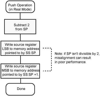
Figure 5-26. Stack Segment
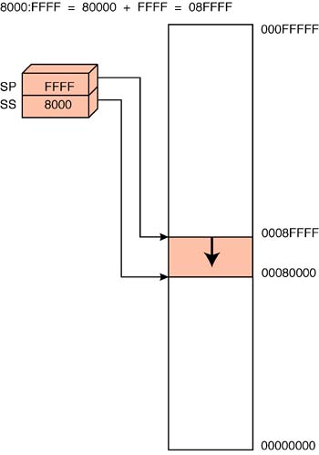
The stack grows downward in memory from the highest memory location in the stack (i.e., the top) towards the segment base address specified in SS.
Popping Data From the Stack
Refer to Figure 5-25 on page 79. To read data back from the stack, the programmer uses the POP instruction. When the programmer executes a POP instruction, such as POP BX, the processor reads two bytes from the stack using the current value in SS:SP to form the memory address:
Continuing the example used earlier, a POP BX causes the processor to read the two bytes (AAh and 55h) from locations 8FFFBh and 8FFFCh and place them into the BX register.
The processor then increments SP by two, so SS:SP are now pointing at 8000:FFFD.
A subsequent POP AX causes the processor to read the two bytes (12h and 34h) from locations 8FFFDh and 8FFFEh and place them into the AX register.
The processor then increments SP by two, so SS:SP are now pointing at 8000:FFFF, the top of the stack. The stack is now empty.
Figure 5-25. Pop Operation in Real Mode

As implemented by the IA32 processors, the stack is a LIFO (Last In, First Out) buffer—the last object in is the first out.
If the programmer attempts to pop more data from the stack than was pushed onto it (referred to as a Stack Underflow), the processor generates a special type of interrupt called a Stack Exception to indicate that the stack is empty. Conversely, if the programmer pushes data onto the stack until the entire segment is full and then attempts to push more data onto the stack (referred to as a Stack Overflow), the processor generates a Stack Exception.
Processor Stack Usage
In addition to the programmer using the stack for temporary storage, the processor also uses it. The following are some (but not all) of the cases where the processor implicitly uses the stack:
When an INT instruction is executed, the processor pushes the current CS, IP and EFlags values onto the stack before jumping to the target interrupt routine.
When a hardware interrupt occurs, the processor pushes the current CS, IP and EFlags values onto the stack before jumping to the target interrupt service routine.
When a software exception occurs, the processor pushes the current CS, IP and EFlags values onto the stack before jumping to the target exception handler. For some exception types, an error code is also pushed onto the stack.
When the processor executes a CALL instruction, it pushes the current IP (for a near CALL) or CS:IP (for a far CALL) values onto the stack before jumping to the target routine.
Accessing the DS Data Segment
Data is typically read from and written to the DS data segment using MOV instructions. The programmer first loads the DS register with the start address of the data segment in memory. This is accomplished using a MOV or LDS instruction. When loading the DS register using a MOV instruction, the data must first be moved into the AX register and then copied into the DS register:
mov ax, 4500
mov ds, ax
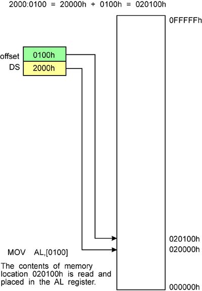
The data segment now starts at location 45000h. The data segment pointed to by the DS register is the default data segment. In this example (see Figure 5-27 on page 83),
mov ax, 4500
mov ds, ax
mov ax, [0100]
Figure 5-27. Example Data Segment Access

the contents of locations 45100h and 45101h are moved into the AX register by the third instruction. The 16-bit offset is enclosed within the brackets while the data segment to be used isn't explicitly specified in this instruction. The processor therefore uses the default data segment, DS, to calculate the physical memory address to be accessed. In Real Mode, it is illegal to specify an offset (the portion within the brackets) value greater than FFFFh. This means that the data segment is limited to 64KB in length in Real Mode. This is one of the drawbacks to Real Mode.
Accessing the ES/FS/GS Data Segments
The following code is used to illustrate the process of accessing data segments other than DS:
mov ax, 1000
mov ds, ax
mov ax, 2000
mov es, ax
mov ax, 3000
mov fs, ax
mov ax, 4000
mov gs, ax
mov bl, [0002]    ;move from ds data segment
mov bh, es:[0002] ;move from es data segment
mov cl, fs:[0002] ;move from fs data segment
mov ch, gs:[0002] ;move from gs data segment
The first memory read moves one byte from location 10002h into the BL register. The second memory read moves one byte from location 20002h into the BH register. The third memory read moves one byte from location 30002h into the CL register. The fourth memory read moves one byte from memory location 40002h into the CH register. ES:, FS: and GS: are referred to as segment overrides. They instruct the processor to access the specified data segment rather than the default data segment (DS).
In all cases, the offset specified within the brackets may not exceed FFFFh when in Real Mode. All segments are therefore restricted to 64KB in size when in Real Mode.
An Example
Figure 5-28 on page 86 illustrates the use of the segment registers in Real Mode. The figure assumes that the following code has already been executed in Real Mode:
at location 0600:0050, the following instruction:
 jmp f000:0100             ;cs = f000, ip = 0100
starting at location f000:0100, the following instructions:

 mov ax, d000
 mov ds, ax     ;ds = d000
 mov ax, a320
 mov ss, ax     ;ss = a320
 mov ax, 7200
 mov es, ax     ;es = 7200
 mov ax, 3000
 mov fs, ax     ;fs = 3000
 mov ax, 1000
 mov gs, ax     ;gs = 1000
Figure 5-28. Example Usage of Segment Registers in Real Mode
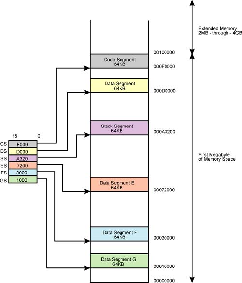
When the processor executes the far jump instruction fetched from memory location 0600:0050 (06050h), the CS register is set to F000h and the IP register to 0100h. As a result, the processor fetches its next instruction from memory location 000F0100h. The series of instructions starting at this location causes the values indicated in the figure to be moved into the stack and data segment registers. The figure illustrates how the processor then uses the segment registers to identify the six segments of memory space.
Accessing Extended Memory in Real Mode
It is possible to access a small amount of extended memory (memory above 1MB) while in Real Mode. Consider the following example:
mov ax,ffff    ;ffffh to ax
mov ds,ax      ;transfer ffffh to ds
mov al,[0010]  ;transfer contents of memory
               ;location ffff:0010 into al
In order to form the physical memory address to place on the FSB when executing the third instruction, the processor appends the digit zero to the lower end of the DS data segment value (FFFFh) to point to the start address of the data segment (FFFF0h). It then adds the offset (0010h) to the data segment start address to create the physical memory address:
      DS + 0h =            FFFF0h
      Offset =              0010h

Physical memory address = 100000h
The processor then performs a memory read transaction, driving the resultant physical memory address, 00100000h, onto the FSB. Notice that the 21st address bit, A[20], is a one. The processor is addressing the first memory location of the second megabyte of memory address space. This is extended memory (i.e., memory above the first MB of memory space) and the processor is addressing it in Real Mode!
Now consider this example:
mov ax,ffff     ;ffffh to ax
mov ds,ax       ;transfer ffffh to ds
mov al,[ffff]   ;read byte from memory address
                ;ffff:ffff into al
As before, in order to form the physical memory address to place on the FSB when executing the third instruction, the processor places a 0h on the lower end of the DS data segment value (FFFFh) to point to the start address of the data segment (000FFFF0h). It then adds the offset (FFFFh) to the data segment start address to create the physical memory address:
      DS + 0h =            FFFF0h
      Offset =              FFFFh

Physical memory address =  10FFEFh
The processor then performs a memory read transaction, driving the resultant physical memory address, 0010FFEFh, onto the address bus. With the value FFFFh in the segment register and by supplying any offset in the range 0010h through FFFFh, any extended memory location from 00100000h through 0010FFEFh can be accessed. A total of 65520d extended memory locations can be accessed while still in Real Mode.
This method is used by many DOS memory management programs to access extended memory while remaining in Real Mode. This memory area is usually referred to as the High Memory Area (HMA).
Note that the code fragments shown earlier can be executed on an 8088/8086 processor (these processors only had a 20-bit address bus consisting of A[19:0]). The results are different, however, when the code is executed on a post 8088/8086 processor (which have more than 20 address signals lines). If an 8088/8086 processor executes the code, address bit A[20] will not be high (because the 8088/8086 processors do not implement address lines above A[19]. Therefore, the 8088/8086 produces an address that is between 00000000h and 0000FFEFh for the examples shown earlier. This is called address or segment wraparound. The address space of the segment wraps around from the highest physical addresses to the lowest physical addresses.
Some programs written for the 8088/8086 may depend on segment wraparound to access data in the low addresses, such as the Interrupt Table or the BIOS data area. If these programs are executed on a post-8088/8086 processor, they do not operate correctly because they aren't accessing the expected memory locations. In order for machines based on post-8088/8086 processors to be compatible with such old code, the processor's A[20] address output must be forced to zero to simulate the address generated by the 8088/8086.
Figure 5-29 on page 89 illustrates the 286 processor implemented in an IBM PC-AT compatible machine. Note that address bit A[20] was set to one when a segment value of FFFFh and offsets larger than 000Fh were used. Therefore, only A[20] needs to be masked. A[23:21] are not set to one when executing the old code.
Figure 5-29. A20 Gate

This discussion assumes that the system is a PC-compatible and the processor is a 286 or 386. External to the processor on the system board, A[20] is connected to one input of an AND gate. The other input of the AND gate is supplied by a signal called A20MASK#. The output of the AND gate becomes the A[20] address bit that is broadcast with the rest of the processor's address to the system. If A20MASK# is asserted (i.e., zero), the AND gate's output (i.e., the system's A[20] bit) is forced to zero, thereby simulating an address generated by an 8088/8086. In early PC-compatible machines, the A20MASK# signal was originated by the keyboard controller under software control. Alternately, it can also be generated by intercept logic that watches for commands issued to the keyboard controller to raise or lower this line.
Big Real Mode
Post-286 processors can address up to 4GB of memory space while in Real Mode, so long as they have (at least once) been switched to Protected Mode and back to Real Mode since the last reset. This is sometimes referred to as Big Real Mode, Flat Real Mode, Real Big Mode and UnReal Mode.
After temporarily switching to Protected Mode, software sets up a segment descriptor table entry (in the Global Descriptor Table—the GDT) that describes a data segment starting at location 0 and with a length (i.e., a limit) of 4GB (see “Intro to Segmentation in Protected Mode” on page 109). Software then loads one or more of the data segment registers (DS, ES, FS and GS) with a value that selects this descriptor, thereby causing the processor to load the invisible part of the segment register (i.e., its associated segment cache register) with the new start address and length. When the switch is made back to Real Mode, as long as the programmer doesn't load a new value into the respective data segment register(s), the previous segment definition holds true. This permits the programmer to access any location within the 4GB data segment. If a new value is loaded into a data segment register, the new base address goes into effect, but the limit (i.e., the segment size) that was loaded while in Protected Mode is not modified. The limit will only be changed under the following circumstances:
If the processor is switched back into Protected Mode and the data segment register is loaded with a value that selects a descriptor defining a different length.
If the processor is reset, all segment lengths (i.e., limits) revert back to 64KB.
If the processor is placed in VM86 Mode, all segment lengths (i.e., limits) revert back to 64KB.
This method cannot be used for the code or stack segments, however. In Real Mode, code fetches from the code segment are performed using the CS:IP register pair and IP is a 16-bit register, thereby restricting the code segment to a length of 64KB. Likewise, stack accesses are performed using the SS:SP register pair and SP is a 16-bit register, thereby restricting the stack segment to a length of 64KB.
The 286 lacked this capability (because it could not be switched from Protected to Real Mode without resetting the processor, thus setting the contents of the invisible part of the segment register to values restricting the processor to accesses within the first meg of memory space).