
Data Bus Parity
Introduction
Table 51-3 on page 1271 defines the data signal lines that each of the four data parity bits are associated with.
| Data Parity Signal | Provides even parity for the overall pattern consisting of: |
|---|---|
| DP0# |
|
| DP1# |
|
| DP2# |
|
| DP3# |
|
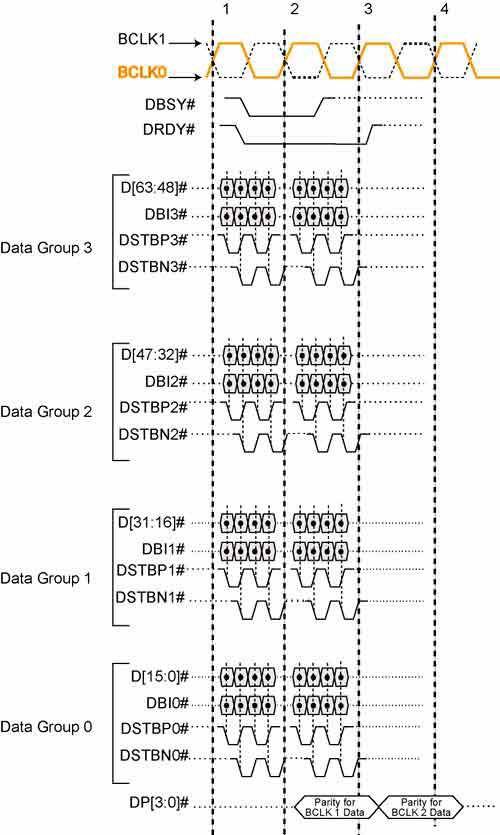
As shown in Figure 51-15 on page 1272, the four parity bits for each 32-byte block of data are driven in the BCLK cycle immediately following the BCLK cycle in which the 32-byte block of data is driven.
In the figure, the device sourcing the data takes ownership of the Data Bus at the start of BCLK cycle 1 by asserting DBSY#.
It also immediately starts sourcing the data and the data strobes and asserts DRDY# to indicate it is doing so.
During BCLK cycle 1, the device receiving the data uses the falling-edges of the data strobes to latch the first 32-byte block during BCLK cycle 1.
The receiving device samples DRDY# asserted at the start of BCLK cycle 2, validating the data received in the previous BCLK cycle.
In BCLK cycle 2, the device sourcing the data keeps DRDY# asserted and immediately starts sourcing the data and the data strobes and asserts DRDY# to indicate it is doing so.
During BCLK cycle 2, the device receiving the data uses the falling-edges of the data strobes to latch the second 32-byte block.
The receiving device samples DRDY# asserted at the start of BCLK cycle 3, validating the data received in the previous BCLK cycle.
The receiving device samples DP[3:0]# at the start of BCLK cycle 3. Internally, the device compares the actual four parity bits to those it computed based on the first 32-byte data block it received at the end of BCLK cycle 1. Refer to “ChipSet Data Phase Parity Checking and Reporting” on page 1273 and “Processor Data Phase Parity Checking and Reporting” on page 1274.
Figure 51-15. Data Phase Parity
ChipSet Data Phase Parity Checking and Reporting
Refer to Figure 51-16 on page 1274. The example system shown is a PCI Express-based system and the device that connects the processors to the remainder of the system is referred to as the Root Complex. In a PCI or a PCI-X based system, it is referred to as the North Bridge or as the Memory Control Hub (MCH). The device that connects the processors to the remainder of the system is part of the chipset.
When a FSB agent other than the chipset (e.g., a processor) initiates a transaction on the FSB, the chipset may or may not check the Data Phase parity bits for correctness. Many chipsets designed for low- and medium- range systems do not. Some high-end chipsets, however, do check for correct Data Phase parity. The actions taken by such a chipset in the event of a Data Phase parity error is chipset design-specific. As an example, some high-end Intel® chipsets take the following actions:
The chipset receives a 32-byte block of data.
The chipset internally calculates the four expected parity bits based on the information received.
The four parity bits just latched are compared to the calculated parity bits:
- If they are the same, the data did not suffer in-flight corruption and the chipset will not report an error.
- If the calculated and actual parity bits disagree, the chipset causes an error signal to be asserted:
- In some chipsets, the ICH (IO Control Hub) chipset member is instructed to send an NMI (Non-Maskable Interrupt) to the processor. This causes the processor to execute the NMI handler routine which checks a chipset status register to determine the cause of the error, reports the error to the end-user, disables interrupt recognition and halts the processor.
- In some chipsets, the MCH asserts MCERR# (Machine Check Error) to the processor. This causes the processor to log an error in its Machine Check Architecture error logging registers and, if the processor is enabled to do so (via CR4[MCE]), generate a Machine Check exception. The MC handler is then executed and checks a chipset status register to determine the cause of the error, reports the error to the end-user, disables interrupt recognition and halts the processor.
Processor Data Phase Parity Checking and Reporting
Whether or not a processor is enabled to check the Data Phase parity when a FSB transaction is initiated by another agent is controller by bit 1 in the EBC_Soft_Poweron MSR (see Figure 51-17 on page 1275). If this capability is enabled, the processor takes the following actions:
The processor receives a 32-byte block of data.
The processor internally calculates the four expected parity bits based on the information received.
The four parity bits just sampled are compared to the calculated parity bits:
- If they are the same, the data block did not suffer in-flight corruption and the processor will not report an error.
- If the calculated and actual parity bits disagree, the processor logs the error as a hard failure (rather than as a correctable error) in its Machine Check Architecture error logging register set. If the processor is enabled to do so (via CR4[MCE]), it also generates a Machine Check exception.
Parity When Transferring a Sub-Block
In a BCLK cycle wherein less than 32-bytes (four qwords) are being transferred, the parity bits still cover four chunks worth of data (Intel®'s name for qwords). As an example, if two qwords are being transferred (as shown in Figure 51-2 on page 1250), valid data is driven during the transfer of the first two qwords and all of the data lines are set high (deasserted) during the transfer of what would normally be the transfer of the next two qwords of a 32-byte block. The agent receiving the data knows the data transfer length, so it only uses the first two qwords of data, but it factors all four qwords into generating the expected parity bits that will be compared to the actual parity bits.