
Load μops
The Load Buffers
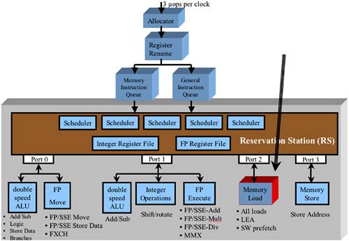
When a load μop arrives at the Allocator stage of the instruction pipeline (see “The Allocator” on page 938), the Allocator reserves one of the processor's 48 Load Buffers to handle the load when it is subsequently dispatched for execution. If Hyper-Threading is enabled, the 48 Load Buffers are partitioned into two groups of 24 buffers each and each group is reserved for the use of one of the logical processors.
See Figure 41-1 on page 1064. Port 2 supports the dispatch of one load operation per cycle. When a load μop is executed by the Load execution unit, the load request is placed in one of Load Buffers and remains there until one of the following becomes true:
The load μop is completed, retired, and deallocated.
Loads from WC, WP, WT and WB memory can be speculatively executed (a speculative load is a load that lies beyond a conditional branch μop that has not yet been executed). If, when the conditional branch μop is subsequently executed it is determined that one or more speculative loads that lie beyond the branch should not have been executed, the contents of those Load Buffers are discarded and those Load Buffers become available to handle additional load μops. See “The Definition of a Speculatively Executed Load” on page 1067.
Loads from Cacheable Memory
The types of memory that the processor is permitted to cache from are WP, WT and WB memory (as defined by the MTRRs and the PTE or PDE).
When the core dispatches a load μop, the μop is placed in the Load Buffer that was reserved for it in the Allocator stage. The memory data read request is then issued to the L1 Data Cache for fulfillment:
If the cache has a copy of the line that contains the requested read data, the read data is placed in the Load Buffer.
If the cache lookup results in a miss, the request is forwarded upstream to the L2 Cache.
If the L2 Cache has a copy of the sector that contains the requested read data, the read data is immediately placed in the Load Buffer and the sector is copied into the L1 Data Cache.
If the cache lookup results in a miss, the request is forwarded upstream to either the L3 Cache (if there is one) or to the FSB Interface Unit.
If the L3 Cache has a copy of the sector that contains the requested read data, the read data is immediately placed in the Load Buffer and the sector is copied into the L2 Cache and the L1 Data Cache.
If the lookup in the top-level cache results in a miss, the request is forwarded to the FSB Interface Unit.
When the sector is returned from memory, the read data is immediately placed in the Load Buffer and the sector is copied into the L3 Cache (if there is one), the L2 Cache, and the L1 Data Cache.
The processor core is permitted to speculatively execute loads that read data from WC, WP, WT or WB memory space (see “The Definition of a Speculatively Executed Load” on page 1067).
Loads Can Be Executed Out-of-Order
The following code fragment reads the contents of four memory-based variables into four of the processor's registers. The description that follows assumes that all four of the memory variables are in cacheable memory:
mov  eax,mem1
mov  ebx,mem2
mov  ecx,mem3
mov  edx,mem4
---
Prior to the advent of the P6 processor family, these instructions would be executed in strict program order. The P6 and Pentium® 4 family processors, however, utilize out-of-order execution strategies:
The first load μop is dispatched to its assigned Load Buffer and that Load Buffer submits the read request to the L1 Data Cache.
If the first load μop resulted in a cache miss, the read request is forwarded upstream to the L2 Cache for fulfillment.
The processor core does not stall. Rather, the memory μop scheduler sees additional loads awaiting execution, so it will immediately dispatch the second load to its assigned Load Buffer.
That Load Buffer submits the read request to the L1 Data Cache.
If the second load μop resulted in a cache miss, the read request is forwarded upstream to the L2 Cache for fulfillment.
The processor core can continue to dispatch additional loads to their respective Load Buffers. However, if the L1 Data Cache experiences more than four cache misses it signals a stall to the Load Buffer logic. No new load requests can be submitted to the cache until at least one of the previous misses has been fulfilled.
Loads are not necessarily executed in order with reference to store μops or to the SFENCE instruction (see “The SFENCE Instruction” on page 1084).
The L1 Data Cache Implements Squashing
If a load causes an L1 Data Cache miss, the request is forwarded upstream to the L2 Cache for fulfillment. The memory instruction scheduler will continue to dispatch additional loads to their respective Load Buffers. If any of the subsequently dispatched loads requires data from the line which has already been requested from the L2, the L1 Data Cache does not issue an additional request for the same line to the L2 Cache. When the line is returned from the L2 cache, it is used to satisfy all of the loads that requested data from that line. This is referred to as squashing multiple requests for the same line into just one request.
Loads from Uncacheable Memory
The uncacheable memory types are UC and WC (as defined by the MTRRs and the PTE or PDE).
When the core dispatches a load μop, the read request is placed in the Load Buffer that was reserved for it in the Allocator stage. The memory data read request is submitted to the processor's caches as well. In the event of cache hit, the cache line is evicted from the cache. The request is issued to the FSB Interface Unit. A Memory Data Read transaction is performed on the FSB to fetch just the requested bytes from memory. When the data is returned from memory, the read data is immediately placed in the Load Buffer.
The processor core is not permitted to speculatively execute loads that read data from UC memory space (see “The Definition of a Speculatively Executed Load” on page 1067).
The Definition of a Speculatively Executed Load
Consider the following code fragment:
 sub  eax,ebx
 je   bypass        ;jump to bypass if result was zero
 mov  eax,mem1      ;read memory variable into eax
 mov  ebx,mem2      ;and another variable into ebx
bypass:
If the memory type of the data variables is WC, WP, WT, or WB, the processor core is permitted to speculatively execute the two load instructions before the conditional branch instruction is executed. The data that is returned is placed in the two Load Buffers that were reserved for the two read requests. If the conditional branch instruction jumps around the two loads when it is executed, the loads should not have been executed. In that case, the processor core invalidates the two Load Buffers and the EAX and EBX registers are not loaded with the two memory variables.
If the attempted speculative execution of a load would result in a Page Fault exception (i.e., the Present bit in the selected PTE or PDE is cleared to zero), the processor will not complete the load. Rather, it will wait until the upstream conditional branch has executed and it has been established that the load should be executed.
Replay
Replay of μops Dependent on a Load
The instruction scheduler may detect one or more μops in the scheduler queues that, when executed, will use the data returned by a load μop into a processor register. The scheduler will dispatch the load μop for execution and, working on the assumption that it will obtain the read data quickly from the L1 Data Cache, may also dispatch one or more μops that are dependent upon the load operation (i.e., operations that will use the read data returned from the L1 Data Cache).
If may come to pass, however, that the load results in an L1 Data Cache miss. In this case, the dependent μops will not have access to the register data they require until the read data is supplied by the L2 Cache. When the read data is finally placed in the Load Buffer, the scheduler re-executes the dependent μops successfully.
Replay of Loads Dependent on a Store
Loads are scheduled asynchronously to store μops. A load may require data produced by a store μop that precedes the load in the program flow. The core may execute the load prior to the store. In this case, the load would have to be re-executed again after the store μop completed execution.
It should be noted that this is one of the areas that was improved with the advent of the 90nm version of the Pentium® 4 (code named Prescott). See “The Pentium® 4 Prescott” on page 1091 for more information.
Loads and the Prefetch Instructions
Introduced in the Pentium® III processor as part of the SSE instruction set, the PREFETCHh instructions can improve the completion time for subsequently executed load instructions. Executing a PREFETCHh instruction causes the processor to fetch a line into a processor cache before subsequent load μops will request data from that line. See “Overlapping Data Prefetch with Program Execution” on page 773 for a detailed description of the PREFETCHh instructions.
The LFENCE Instruction
General
Consider the following code fragment:
mov  eax,10
mov  ebx,memioport1   ;read from memory mapped IO port 1
mov  edx,memioport2   ;read from memory mapped IO port 2
xor  eax,edx
mov  ecx,memioport3   ;read from memory mapped IO port 3
This example performs reads from three memory mapped IO ports in a device adapter and assumes that the ports are in a UC memory range. Proper operation of the example adapter requires that the three memory data read transactions be performed in strict program order. Since the processor can execute loads in any order, this code fragment may result in an improper sequence of the reads on the FSB. The Load Fence instruction (first implemented in the Pentium® 4 processor) fixes this situation:
mov  eax,10
mov  ebx,memioport1  ;read from memory mapped IO port 1
mov  edx,memioport2  ;read from memory mapped IO port 2
xor  eax,edx
lfence               ;cannot perform loads beyond fence
                     ;until all prior loads have completed
mov  ecx,memioport3  ;read from memory mapped IO port 3
It should be noted that, while the processor cannot execute loads beneath the fence until all upstream loads have completed, the processor can execute non-load μops beneath the fence before all loads above the fence have completed. In the following example, the programmer has used the CPUID instruction to accomplish the same goal:
mov  eax,10
mov  ebx,memioport1  ;read from memory mapped IO port 1
mov  edx,memioport2  ;read from memory mapped IO port 2
xor  eax,edx
mov  eax,1           ;set up for a CPUID request type 1
cpuid                ;acts as a barrier in the code
mov  ecx,memioport3  ;read from memory mapped IO port 3
CPUID is a serializing instruction (see “Serializing Instructions” on page 1079). The processor cannot execute any μop beneath the fence until all of the μops above the fence have been executed and retired. This causes a significant drop in performance due to the constraint placed on out-of-order execution. Using the LFENCE instruction results in better performance.
Although the example assumed that the memory locations read were in UC memory space, the LFENCE instruction can be used to fence loads from any type of memory space.
LFENCE Ordering Rules
The LFENCE instruction is executed in order with reference to load μops, to other instances of the LFENCE instruction, to instances of the MFENCE instruction (see “The MFENCE Instruction” on page 1089), and to any serializing instructions (e.g., CPUID; see “Serializing Instructions” on page 1079). It is not necessarily executed in order with reference to store μops or to the SFENCE instruction (see “The SFENCE Instruction” on page 1084).
The LFENCE instruction is not necessarily executed in order with reference to PREFETCHh instructions or to any other speculative fetching mechanism (data could be speculative loaded into the cache just before, during, or after the execution of an LFENCE instruction).