
Miscellaneous New Instructions
General
The 130nm Pentium® 4 processor added 144 new instructions to the IA32 instruction repertoire. This is referred to as the SSE2 instruction set. Of these, the author has chosen to discuss the following instructions separately in this section and the remainder are covered in “The SSE2 Instruction Set” on page 1332.
The CLFLUSH instruction is covered in “The Cache Line Flush Instruction” on page 1326.
The MFENCE instruction is covered in “The Memory Fence Instruction” on page 1326.
The LFENCE instruction is covered in “The Load Fence Instruction” on page 1326.
The non-temporal store instructions (also referred to as Streaming Stores) are covered in “The Non-Temporal Store Instructions” on page 1327.
The PAUSE instruction is covered in “The PAUSE Instruction” on page 1331.
The branch hints are covered in “The Branch Hints” on page 1332.
The 90nm Pentium® 4 processor added an additional 13 instructions (referred to as the SSE3 instruction set) and they are covered in “The SSE3 Instruction Set” on page 1337.
The Cache Line Flush Instruction
See the description found in Table 40-11 on page 1057. The programmer can determine the processor's cache line size by executing a CPUID request type 1 and examining the second byte returned in the EBX register (see Figure 56-1).
Figure 56-1. The EBX Register After Executing a CPUID Request Type 1

The Fence Instructions
The Memory Fence Instruction
See the description in “The MFENCE Instruction” on page 1089.
The Load Fence Instruction
See the description found in “The LFENCE Instruction” on page 1068.
The Non-Temporal Store Instructions
Introduction
The category of instructions referred as streaming stores or as non-temporal stores was introduced in the Pentium® III processor (see “Streaming Store Instructions” on page 776). The Pentium® 4 processor added four additional streaming store instructions:
They are described in the sections that follow.
The MOVNTDQ Instruction
Refer to Figure 56-2 on page 1328. This instruction is a Store Double Qword to memory using a non-temporal hint. When executed, it moves 16 bytes of data from the specified XMM register into memory. When this instruction is executed, the processor treats the line of memory space being written to as if it were the WC memory type (even though the MTRRs and the PTE or PDE selected by the linear address may designate it as WB memory). Executing this instruction has the following effects:
The 16 bytes from the specified XMM register are placed into the appropriate locations in one of the processor's WC buffers (WCB; see “Stores to WC Memory” on page 1075 for more information) and the start address of the line is also latched into that WCB. The data will be written to memory at a later time when the WCB is written to memory using the FSB.
Assuming that the memory type is WB, the line is not fetched from memory, so none of the disadvantages cited in Table 31-6 on page 777 are experienced.
The processor performs a lookup in its internal caches and, if the line is present in the cache, it is evicted from the cache.
Figure 56-2. The MOVNTDQ Instruction

The memory type (UC or WP) of the region being written to can override the non-temporal hint.
The MOVNTPD Instruction
Refer to Figure 56-3 on page 1329. The instruction name stands for “move packed DP FP values into memory using a Non-Temporal hint”. When executed, it stores the two 64-bit SP FP values packed into an XMM register to memory. The start memory address specified must be aligned on a 16-byte (128-bit) boundary.
Figure 56-3. The MOVNTPD Instruction

When this instruction is executed, the processor treats the line of memory space being written to as if it were the WC memory type (even though the MTRRs and the PTE or PDE selected by the linear address may designate it as WB memory). Executing this instruction has the following effects:
The two 64-bit DP FP numbers supplied from the specified XMM register are placed into the appropriate locations in one of the processor's WC buffers (WCB; see “Stores to WC Memory” on page 1075 for more information) and the start address of the line is also latched into that WCB. The data will be written to memory at a later time when the WCB is written to memory using the FSB.
Assuming that the memory type is WB, the line is not fetched from memory, so none of the disadvantages cited in Table 31-6 on page 777 are experienced.
The processor performs a lookup in its internal caches and, if the line is present in the cache, it is evicted from the cache.
The memory type (UC or WP) of the region being written to can override the non-temporal hint.
The MOVNTI Instruction
Refer to Figure 56-4 on page 1330. This instruction is a Store 32-bit integer to memory using a Non-Temporal hint. When executed, it moves four bytes of data from the specified GPR into memory. When this instruction is executed, the processor treats the line of memory space being written to as if it were the WC memory type (even though the MTRRs and the PTE or PDE selected by the linear address may designate it as WB memory). Executing this instruction has the following effects:
The four bytes from the specified GPR are placed into the appropriate locations in one of the processor's WC buffers (WCB; see “Stores to WC Memory” on page 1075 for more information) and the start address of the line is also latched into that WCB. The data will be written to memory at a later time when the WCB is written to memory using the FSB.
Assuming that the memory type is WB, the line is not fetched from memory, so none of the disadvantages cited in Table 31-6 on page 777 are experienced.
The processor performs a lookup in its internal caches and, if the line is present in the cache, it is evicted from the cache.
Figure 56-4. The MOVNTI Instruction

The memory type (UC or WP) of the region being written to can override the non-temporal hint.
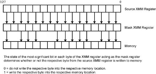
The MASKMOVDQU Instruction
General
Refer to Figure 56-5 on page 1331. When executed, this instruction uses the bit mask specified in one XMM register to determine which of the 16 bytes in another XMM register are to be written to memory. Bit 7 in each byte of the specified XMM mask register indicates whether the corresponding data byte from the source XMM register will be written to memory (1 = write the byte to memory; 0 = do not write it to memory). The memory address is specified in the DS:DI (if executing in 16-bit mode) or the DS:EDI register pair (if executing in 32-bit mode):
- The specified bytes from the source XMM register are placed into the appropriate locations in one of the processor's WC buffers (WCB; see “Stores to WC Memory” on page 1075 for more information) and the start address of the line is also latched into that WCB. The data will be written to memory at a later time when the WCB is written to memory using the FSB.
- Assuming that the memory type is WB, the line is not fetched from memory, so none of the disadvantages cited in Table 31-6 on page 777 are experienced.
- The processor performs a lookup in its internal caches and, if the line is present in the cache, it is evicted from the cache.
The information cited in “The MASKMOVQ Instruction” on page 782 also applies to this instruction.
When a Mask of All Zeros Is Used
The processor's behavior when a mask of all 0s is specified is as follows:
- No data is written to memory.
- Signaling of breakpoints (code or data) is not guaranteed; different processor implementations may or may not signal breakpoints.
- Exceptions associated with addressing memory and Page Faults may still be signaled (implementation dependent).
- If the destination memory is mapped as UC or WP, enforcement of the rules for these memory types is not guaranteed (it is reserved) and is implementation-specific.
The PAUSE Instruction
See the discussion in “Thread Synchronization” on page 1001.
The Branch Hints
Two hexadecimal instruction prefixes were added (2Eh and 3Eh). When a conditional branch instruction is prefixed by one of these hints, it tells the processor's branch prediction logic whether to predict the branch taken or not taken. The prefixes can only be used with the conditional branch instructions and there are no mnemonics for the branch hints:
2Eh— Predict the branch not taken.
3Eh— Predict the branch taken.